 |
|
|
|
Site Navigation
Projects & Information
»General Information»Wind turbine Projects »The F&P Smartdrive »Electronic projects »Microcontroller projects »Miscellaneous Kits & Parts
»Basicly Natural Pty Ltd»PVC & Aluminium blades »Scale model farm windmills »Price Watch Discussion Forums
Handy Links
»Wind»Solar »Electric Vehicles »Electronics »Micro Controllers »General Interrest About TheBackShed Getting Started Privacy Policy |
Now the step by step. Prepare your circuit artwork on the computer and print it off onto plain white paper in a high quality setting for the printer. Print in black ink. The image needs to be printed in a mirror image to what the copper view will end up to be. (back to front) Most pcb design artwork packages will print the bottom side of a board (as used for single sided boards) in a mirror image as standard. The reason for this is we need to place the ink side down onto the pcb for exposure. With the black ink in contact with the uv sensitive film no light can reach that part of the uv coating and will not be exposed. Cut the image from the paper sheet and sparingly apply a light coat of cooking oil (vegetable oil) over the Back side of the printed paper with a tissue. Rub it gently to get the oil to work into the paper. You will see the printed image appear quite clearly through the paper. Clean off any excess oil with a clean tissue. ( It pays to discard the paper after use and print a new one if several days has pass after oiling it)
Cut the board to size ( a hacksaw works) and clean up the edges so no copper burs remain. Remove the plastic film covering the board. This will expose the green uv sensitive film on the board. Try to do this under low light levels and preferably with a incandescent light as this has no real UV light spectrum. (fluros do)
Align the printed artwork over the board ink side down Place a sheet of glass over the top of the paper to hold it firmly in contact with the pcb. Check that all is still aligned correctly, Start the uv light exposure. I find 10 passes (5 ups and backs) of the uv leds travelling at 300mm/min (slow) at a height of 100mm from the circuit board gives a good print. If the leds are used stationary than exposure time is 10 times less, as the leds only cover a strip as they travel up and back along the board. My uv light scanner was made from the carriage section gutted from an old inkjet printer and Uv led clusters. ( 2 rows of single leds work just as well)
It is important to have the leds start off the board and travel the length of the board and off the other end before they reverse and return, otherwise the ends where it stops and reverses will get double exposure and wont develop uniform.
Once the exposure is started, wait till its completed 10 passes and has switched itself off. Remove the pcb and attach a piece of electrical tape to the backside of pcb with one end wrapped back around some plastic coated wire for a handle to hold/hang it from. (Not such a good method for doublesided boards. Works well on single sided.)
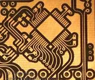
Place the pcb in the caustic solution and gently keep it moving in the solution. The image will start to appear this may be quick or slow depending on the strength and the temperature of the caustic solution. You will need to ensure all the green coating between the tracks has developed away as a light hard to see film remaining will make for a poor etch. I find that a fine line along the edge on the artwork can give a good indication when over developing is happening, as this line will tend to be noticed to disappear first. Rinse the board and inspect a few times during developing and you will soon see when it has developed fully. After developing the board should look something like this.
|
||