
|
|
Forum Index : Microcontroller and PC projects : PicoMite RP2350B DIL Development board, 16Mb flash + 8 MB PSRAM
| Page 1 of 4 |
|||||
| Author | Message | ||||
| matherp Guru Joined: 11/12/2012 Location: United KingdomPosts: 11636 |
Pico2350DIL.zip This file contains the design files, schematics, gerbers, BOM, and Pick&place files for two versions of the 64-pin dual-in-line RP3250B development board. These boards can now be made by JLC who have stock of the RP2350B processors. The boards include positions for the APS6404L-3SQR-SN PSRAM chips but these are currently out of stock at JLC. See the link for the ones I purchased. They are SOP8 packages so easy enough to hand solder. V1.1 is the board I have just had made V1.2 is a cut down board designed to minimise costs (costed at $49 for 5 at JLC) V1.1 is tested to 396MHz without the PSRAM and 378MHz with PSRAM as well as at 1280x720 resolution HDMI (372MHz). IMPORTANT: before powering up one of these boards the potentiometer that sets the DVDD voltage should be adjusted. Connect a multimeter across the test points TP1 and DVDD and adjust the resistance to set the voltage - DVDD = 1.0V + 0.1V per 6kohm For overclocking to 378MHz you will need a voltage of 1.4-1.5V. NB: the firmware already does this using the internal regulator in the RP2350 so this is within known limits. The board breaks out all 48 GPIO pins on the RP2350B except GP0 which is reserved for the PSRAM chip select. By default with the PicoMite firmware variants the heartbeat is not enabled for the RP2350B but you can use OPTION HEARTBEAT ON to enable it if required on GP25. V1.1 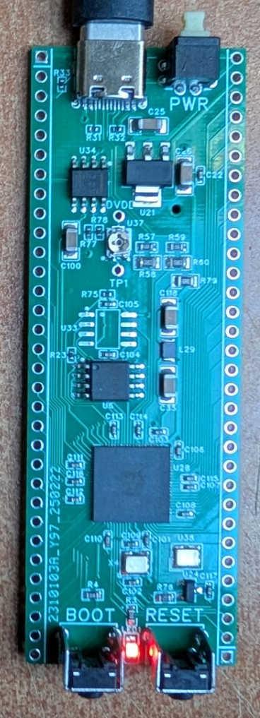 V1.2 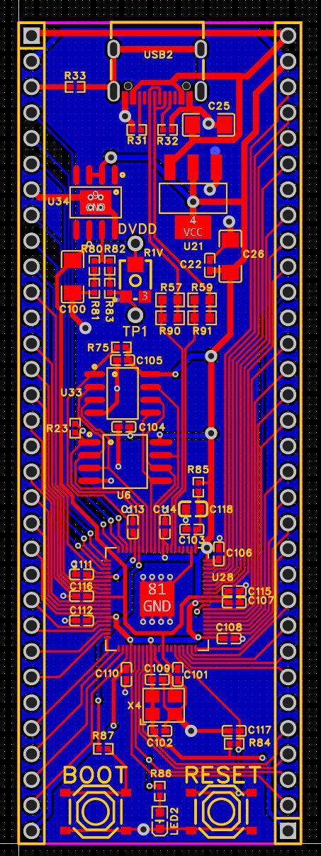 Footnote added 2025-03-01 03:14 by matherp If using the V1.2 files in this post make sure you untick U34/U25 which are the 32-pin headers as they will install them on the wrong side. UPdate versions posted below Footnote added 2025-03-01 03:15 by matherp U35/U36 |
||||
| dddns Guru Joined: 20/09/2024 Location: GermanyPosts: 874 |
I would like to attach a ssd1963 to it. Is that possible? |
||||
| lizby Guru Joined: 17/05/2016 Location: United StatesPosts: 3811 |
Is that 5 assembled boards for $49 (excepting PSRAM)? PicoMite, Armmite F4, SensorKits, MMBasic Hardware, Games, etc. on FOTS |
||||
| matherp Guru Joined: 11/12/2012 Location: United KingdomPosts: 11636 |
Not with current firmware as I'm using GP0. However I will add flexibility to allow this in the near future Yes, plus p+p of course and any relevant local taxes. |
||||
| lizby Guru Joined: 17/05/2016 Location: United StatesPosts: 3811 |
When I go to order from JLCPCB, after downloading the file and clicking Assembly, it says (in effect) dimensions not given. I scroll up and have nothing for X & Y dimensions. What are they? PicoMite, Armmite F4, SensorKits, MMBasic Hardware, Games, etc. on FOTS |
||||
| matherp Guru Joined: 11/12/2012 Location: United KingdomPosts: 11636 |
Don't understand works perfectly for me - just tested again. Make sure you untick U35/U36 otherwise they will install the headers on the wrong side - edit them out of the BOM and P+P. I'll post updates when I've done it. Edited 2025-03-01 03:09 by matherp |
||||
| matherp Guru Joined: 11/12/2012 Location: United KingdomPosts: 11636 |
Files updated to remove the headers Pico2350DIL.zip |
||||
| lizby Guru Joined: 17/05/2016 Location: United StatesPosts: 3811 |
I misunderstood and sent the whole original zip file. Have now submitted the 3 relevant files from that file--gerbers, BOM, and pick & place. All successful--though I had to affirm a whole new list of items that I would comply with, including not re-exporting to Russia. Merchandise Total $49.84 Shipping Estimate $7.81 Coupon Discount -$9.00 Paypal Payment fee $0.50 Sales Tax $2.95 Grand Total $52.10 Now I will have to see if there are complications or charges from the U.S. tariffs to go into place on March 4 on imports from China. I might in theory have to pay an additional 25% plus 25%, though how I would pay and how the package would get to me may not yet be determined. ~ PicoMite, Armmite F4, SensorKits, MMBasic Hardware, Games, etc. on FOTS |
||||
| WhiteWizzard Guru Joined: 05/04/2013 Location: United KingdomPosts: 2991 |
For anyone interested, I have placed an order for a quantity of v1.2 units (without headers, and no PSRAM installed); they should arrive hopefully late next week. For anyone in the UK interested in quickly getting their hands on one of these modules then please PM me as I will have a few spare. Estimate is about £12 per module - this purely covers all costs to land them here in UK (including Duty!) Will be ordering some PSRAM chips too so can solder this SMD part too if required (at cost once again). |
||||
| WhiteWizzard Guru Joined: 05/04/2013 Location: United KingdomPosts: 2991 |
This is to confirm that I have just received the 2350B DIL modules from JLC (they look great Peter!). Because JLC were out of stock of the PSRAM chips, I ordered genuine parts from Mouser; these arrived yesterday so I have everything needed to begin shipping these out. For those of you that have been in touch via PM or email, I will start processing your units today with the intention of dispatching by end of tomorrow (Saturday). For anyone interested, I am selling them at £12 per module as supplied by JLC (plus shipping). As mentioned above, the base module is without the PSRAM chip, and it is also without headers, but I can easily add any of these if required. If you would like one of these useful DIL modules then PLEASE PM me with the following info (this also applies to the members that have already contacted me as I need to know your shipping address!): 1> Whether you want me to add the PSRAM chip (+£1.75) 2> Whether to add header pins (downwards facing) (+£1.50) NOTE: this will increase shipping cost 3> Whether you want MMBASIC installed - if so, which variant. I will simply load the latest version (currently B16, but by the time I post this Peter will probably be on B22  ). ).4> Preferred Shipping method. I will likely use Royal Mail, but the cost is difficult to define exactly. I will simply pass on the cost that I am charged. Special Delivery will be the most expensive for UK destinations at around £7 (regardless of header-pins being installed). Cheapest will likely be around £2 for second class (and without header pins). Will begin with back-log orders, then remaining modules will be on a first come, first served basis........ Footnote added 2025-03-07 20:46 by WhiteWizzard 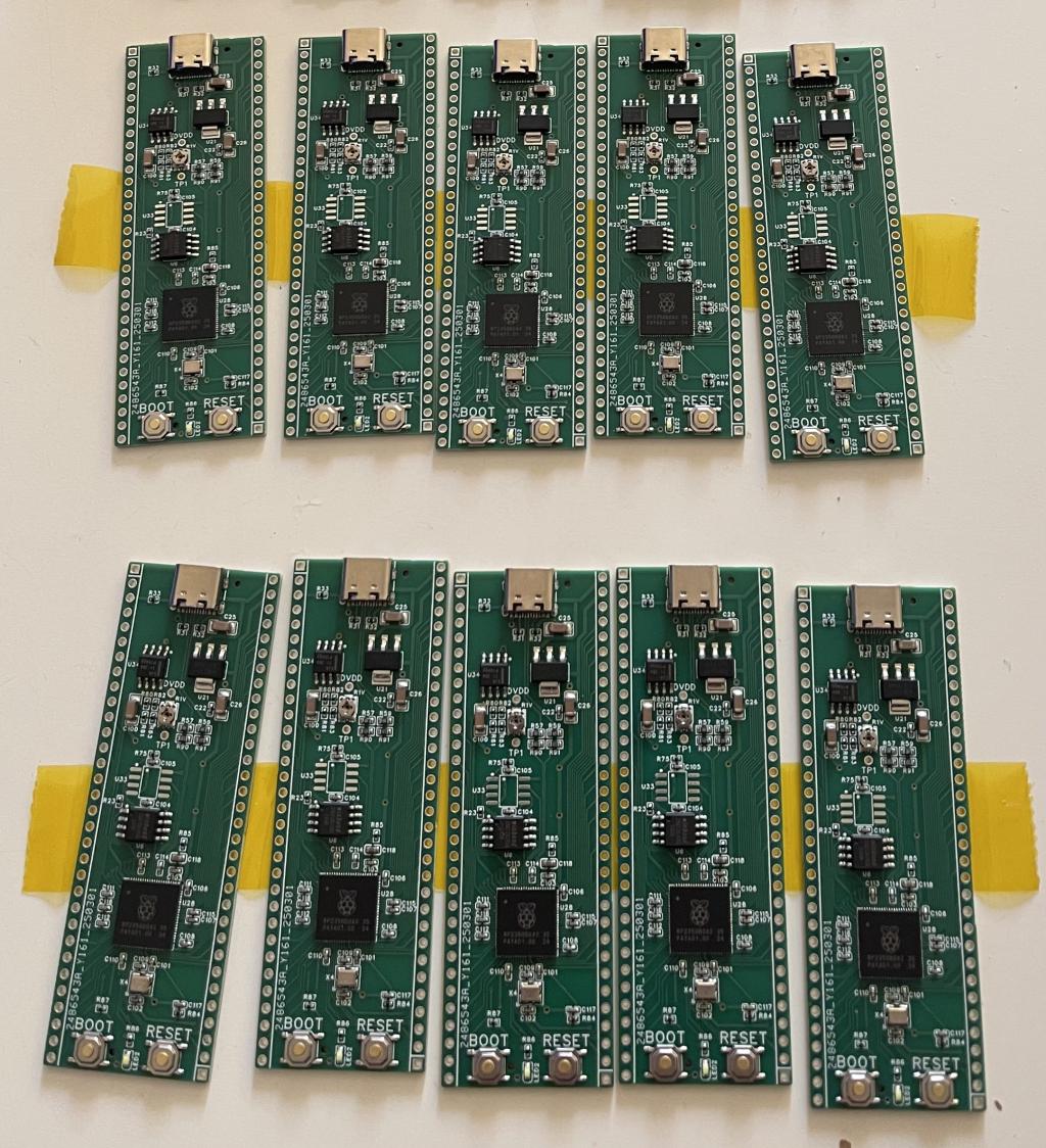 |
||||
| matherp Guru Joined: 11/12/2012 Location: United KingdomPosts: 11636 |
Can I suggest you set the pot before posting. Use a voltmeter between the DVDD test point and GND and set the voltage to 1.3V. This supports 378MHz operation using b16 |
||||
| WhiteWizzard Guru Joined: 05/04/2013 Location: United KingdomPosts: 2991 |
What amazing timing - was just setting it as you were no doubt typing. I set it to 12K and then read your post..... This module will be so useful having every GPIO exposed. Do you have a B17 due out any time today (just asking so I can download the latest firmware) THANKS |
||||
| WhiteWizzard Guru Joined: 05/04/2013 Location: United KingdomPosts: 2991 |
@Peter, FYI - on loading the basic firmware (PicoMiteRP2350V6.00.02b16.uf2), OPTION LIST will show HEARTBEAT PIN GP25 but it won't flash the LED until OPTION HEARTBEAT ON is set (not really a problem). However, on subsequent OPTION LIST it does not show OPTION HEARTBEAT ON. Also to cheekily ask if the OPTION LIST results could be sorted alphabetically please.... Footnote added 2025-03-07 22:05 by WhiteWizzard Correction - If HEARTBEAT is OFF it is listed, but if ON it is not shown in OPTION LIST. Is it easy to make it visible (with ON or OFF) whenever the HEARTBEAT PIN is defined. Ideally if HEATBEAT PIN not defined then the status (ON/OFF) is not shown in the list. |
||||
| Sasquatch Guru Joined: 08/05/2020 Location: United StatesPosts: 385 |
Hi Peter (and fellow shedders) Please Note: I'm not asking for any changes, just thoughts and opinions from you and the community. I have the design up in EasyEDA so I could potentially make a few tweaks to the design at my own risk. I am curious about your choice of GP0 for the PSRAM_SS (chip select). On the one hand GP0 has other established uses going back to MMBASIC on the RP2040. On the other hand, it does leave a 16bit port available on GP32-GP47. This would be especially useful if the PIO access to these GPIO can be sorted. GP47 seems like a natural choice as it hasn't been available on previous hardware designs and thus no established uses for GP47. I notice that on your HDMIUSB reference design you seem to be using GP47. I suppose in the end there is no perfect solution and the decision had to be made. Could a case be made for solder links to "swap" the destination of GP0 and GP47? My other thought was to eliminate the footprint for the PSRAM and mount it "piggy back" style on the FLASH chip (as their pin-outs are identical) and provide a pad near pin1 for the SS. This would reduce the track lengths for the high speed QSPI signals but not be nearly as user friendly for those who don't solder SMT. Your careful layout avoiding sharp corners and vias in the QSPI tracks seems to have mitigated this concern? Any thoughts or opinions from you or the community would be appreciated! -Carl |
||||
| matherp Guru Joined: 11/12/2012 Location: United KingdomPosts: 11636 |
GP47 is much harder to route and the lines need to be kept as short as possible. A selectable link would increase the routing length and if you did that you couldn't then route both to I/O pins as you would have a long routing on the end of PSRAM SS. As you identify I make sure there are no vias in the routes to the flash and PSRAM. I think this is important. You are of course free to modify the design in any way you want but it's on you if the overclock isn't as stable. |
||||
| Mixtel90 Guru Joined: 05/10/2019 Location: United KingdomPosts: 8964 |
Personally I don't like any of the available choices for PSRAM enable, but we are stuck with them! GP0 is probably the best choice of a bad lot for us as it hasn't really got a fixed use in MMBasic, although it is one of the default UART pins in other languages. It's mainly been used as a "convenience" pin" in the past. GP8 is assigned to our default keyboard or console. This can be reassigned but it's a bit of a pain. GP19 is one of the HSTX pins so it would rule out HDMI. GP47 is one of the eight ADC pins, which some people will want now that the problem has been fixed. Mick Zilog Inside! nascom.info for Nascom & Gemini Preliminary MMBasic docs & my PCB designs |
||||
| circuit Guru Joined: 10/01/2016 Location: United KingdomPosts: 307 |
I rubbed the magic lamp and out came a genie (=genius) called Peter. I wished for a DIL board for my 2350. The genie sent me some magic spells and told me to send them to a mysterious place in China with some gold coins. A week later, my wish came true and there they were, lying on the carpet next to the front door. 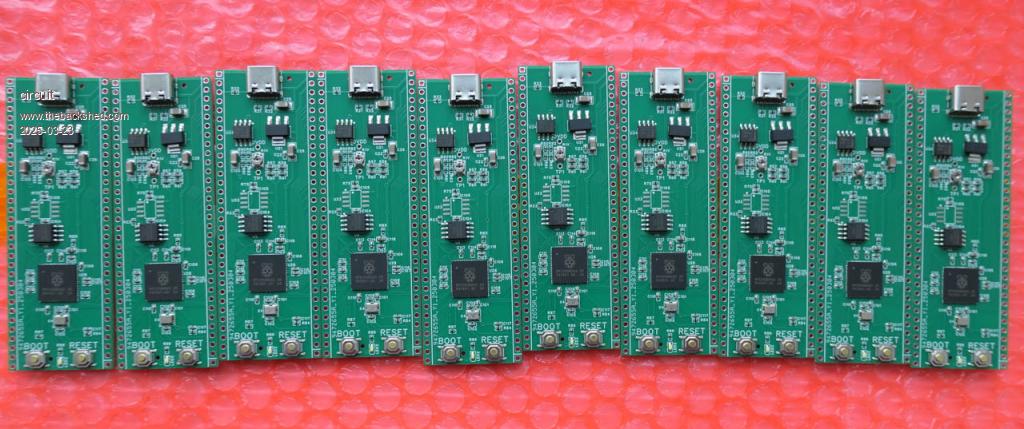 But seriously, Peter, I am totally delighted and thrilled to receive these boards; they were exactly what I had envisioned. My gratitude knows no bounds, thank you. I found that collating all the pin functions/designations for the board from the manual was a little challenging because some come from the 2040 diagram, others from paragraph text and the 5v tolerance from other threads. I think that I have it right and therefore I enclose the mapping diagram below. If anyone has the patience to check this out and proof read it, I would be most appreciative. Corrections or an endorsement that is correct would be great. 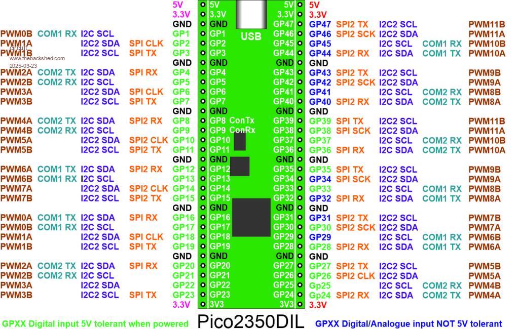 Similarly, if it all correct and there is any space for it in a future manual then i would be delighted to upload a hi-res version in whatever format would be required. Again, Peter, I cannot tell you just how much I value your work. Biggest thanks! Edited 2025-03-23 08:16 by circuit |
||||
| PhenixRising Guru Joined: 07/11/2023 Location: United KingdomPosts: 2003 |
 X 1000 X 1000 |
||||
| matherp Guru Joined: 11/12/2012 Location: United KingdomPosts: 11636 |
GP29,31,32, and 34 are 5V tolerant - RP2350 datasheet page 1321 Attached the data table that specifies pin use - it isn't impossible I've missed something but the definitive reference is RP2350 datasheet pages 18,19 and 20 { 0, 99, "NULL", UNUSED ,99, 99}, { 1, 0, "GP0", DIGITAL_IN | DIGITAL_OUT | SPI0RX | UART0TX | I2C0SDA | PWM0A,99,0}, // pin 1 { 2, 1, "GP1", DIGITAL_IN | DIGITAL_OUT | UART0RX | I2C0SCL | PWM0B ,99,128}, // pin 2 { 3, 99, "GND", UNUSED ,99,99}, // pin 3 { 4, 2, "GP2", DIGITAL_IN | DIGITAL_OUT | SPI0SCK | I2C1SDA | PWM1A ,99,1}, // pin 4 { 5, 3, "GP3", DIGITAL_IN | DIGITAL_OUT | SPI0TX | I2C1SCL | PWM1B ,99,129}, // pin 5 { 6, 4, "GP4", DIGITAL_IN | DIGITAL_OUT | SPI0RX| UART1TX | I2C0SDA | PWM2A ,99,2}, // pin 6 { 7, 5, "GP5", DIGITAL_IN | DIGITAL_OUT | UART1RX | I2C0SCL | PWM2B ,99,130}, // pin 7 { 8, 99, "GND", UNUSED ,99, 99}, // pin 8 { 9, 6, "GP6", DIGITAL_IN | DIGITAL_OUT | SPI0SCK | I2C1SDA | PWM3A ,99, 3}, // pin 9 { 10, 7, "GP7", DIGITAL_IN | DIGITAL_OUT | SPI0TX | I2C1SCL | PWM3B ,99, 131}, // pin 10 { 11, 8, "GP8", DIGITAL_IN | DIGITAL_OUT | SPI1RX | UART1TX | I2C0SDA | PWM4A ,99, 4}, // pin 11 { 12, 9, "GP9", DIGITAL_IN | DIGITAL_OUT | UART1RX | I2C0SCL | PWM4B ,99, 132}, // pin 12 { 13, 99, "GND", UNUSED ,99, 99}, // pin 13 { 14, 10, "GP10", DIGITAL_IN | DIGITAL_OUT | SPI1SCK | I2C1SDA | PWM5A ,99, 5}, // pin 14 { 15, 11, "GP11", DIGITAL_IN | DIGITAL_OUT | SPI1TX | I2C1SCL | PWM5B ,99, 133}, // pin 15 #ifdef HDMI { 16, 12, "HDMI", UNUSED ,99, 99}, // pin 16 { 17, 13, "HDMI", UNUSED ,99, 99}, // pin 17 { 18, 99, "GND", UNUSED ,99, 99}, // pin 18 { 19, 14, "HDMI", UNUSED ,99, 99}, // pin 19 { 20, 15, "HDMI", UNUSED ,99, 99}, // pin 20 { 21, 16, "HDMI", UNUSED ,99, 99}, // pin 21 { 22, 17, "HDMI", UNUSED ,99, 99}, // pin 22 { 23, 99, "GND", UNUSED ,99, 99}, // pin 23 { 24, 18, "HDMI", UNUSED ,99, 99}, // pin 24 { 25, 19, "HDMI", UNUSED ,99, 99}, // pin 25 #else { 16, 12, "GP12", DIGITAL_IN | DIGITAL_OUT | SPI1RX | UART0TX | I2C0SDA | PWM6A ,99, 6}, // pin 16 { 17, 13, "GP13", DIGITAL_IN | DIGITAL_OUT | UART0RX | I2C0SCL | PWM6B ,99, 134}, // pin 17 { 18, 99, "GND", UNUSED ,99, 99}, // pin 18 { 19, 14, "GP14", DIGITAL_IN | DIGITAL_OUT | SPI1SCK | I2C1SDA | PWM7A ,99, 7}, // pin 19 { 20, 15, "GP15", DIGITAL_IN | DIGITAL_OUT | SPI1TX | I2C1SCL | PWM7B ,99, 135}, // pin 20 { 21, 16, "GP16", DIGITAL_IN | DIGITAL_OUT | SPI0RX | UART0TX | I2C0SDA | PWM0A ,99, 0}, // pin 21 { 22, 17, "GP17", DIGITAL_IN | DIGITAL_OUT | UART0RX | I2C0SCL | PWM0B ,99, 128}, // pin 22 { 23, 99, "GND", UNUSED ,99, 99}, // pin 23 { 24, 18, "GP18", DIGITAL_IN | DIGITAL_OUT | SPI0SCK | I2C1SDA | PWM1A ,99, 1}, // pin 24 { 25, 19, "GP19", DIGITAL_IN | DIGITAL_OUT | SPI0TX | I2C1SCL | PWM1B ,99, 129}, // pin 25 #endif { 26, 20, "GP20", DIGITAL_IN | DIGITAL_OUT | SPI0RX | UART1TX| I2C0SDA | PWM2A ,99, 2}, // pin 26 { 27, 21, "GP21", DIGITAL_IN | DIGITAL_OUT | UART1RX| I2C0SCL | PWM2B ,99, 130}, // pin 27 { 28, 99, "GND", UNUSED ,99, 99}, // pin 28 { 29, 22, "GP22", DIGITAL_IN | DIGITAL_OUT | SPI0SCK | I2C1SDA| PWM3A ,99, 3}, // pin 29 { 30, 99, "RUN", UNUSED ,99, 99}, // pin 30 { 31, 26, "GP26", DIGITAL_IN | DIGITAL_OUT | ANALOG_IN | SPI1SCK| I2C1SDA | PWM5A , 0 , 5},// pin 31 { 32, 27, "GP27", DIGITAL_IN | DIGITAL_OUT | ANALOG_IN | SPI1TX| I2C1SCL | PWM5B , 1, 133},// pin 32 { 33, 99, "AGND", UNUSED ,99, 99}, // pin 33 { 34, 28, "GP28", DIGITAL_IN |DIGITAL_OUT| ANALOG_IN| SPI1RX| UART0TX|I2C0SDA| PWM6A, 2, 6},// pin 34 { 35, 99, "VREF", UNUSED ,99, 99}, // pin 35 { 36, 99, "3V3", UNUSED ,99, 99}, // pin 36 { 37, 99, "3V3E", UNUSED ,99, 99}, // pin 37 { 38, 99, "GND", UNUSED ,99, 99}, // pin 38 { 39, 99, "VSYS", UNUSED ,99, 99}, // pin 39 { 40, 99, "VBUS", UNUSED ,99, 99}, // pin 40 #ifndef PICOMITEWEB { 41, 23, "GP23", DIGITAL_IN | DIGITAL_OUT | SPI0TX | I2C1SCL| PWM3B ,99 , 131}, // pseudo pin 41 { 42, 24, "GP24", DIGITAL_IN | DIGITAL_OUT | SPI1RX | UART1TX | I2C0SDA| PWM4A ,99 , 4}, // pseudo pin 42 { 43, 25, "GP25", DIGITAL_IN | DIGITAL_OUT | UART1RX | I2C0SCL| PWM4B ,99 , 132}, // pseudo pin 43 { 44, 29, "GP29", DIGITAL_IN | DIGITAL_OUT | ANALOG_IN | UART0RX | I2C0SCL | PWM6B, 3, 134},// pseudo pin 44 #endif #ifdef rp2350 #ifndef PICOMITEWEB { 45, 30, "GP30", DIGITAL_IN | DIGITAL_OUT | SPI1SCK | I2C1SDA | PWM7A ,99 , 7}, // pseudo pin 45 { 46, 31, "GP31", DIGITAL_IN | DIGITAL_OUT | SPI1TX | I2C1SCL| PWM7B ,99 , 135}, // pseudo pin 46 { 47, 32, "GP32", DIGITAL_IN | DIGITAL_OUT | UART0TX | SPI0RX | I2C0SDA| PWM8A ,99 , 8}, // pseudo pin 47 { 48, 33, "GP33", DIGITAL_IN | DIGITAL_OUT | UART0RX | I2C0SCL| PWM8B ,99 , 136}, // pseudo pin 48 { 49, 34, "GP34", DIGITAL_IN | DIGITAL_OUT | SPI0SCK | I2C1SDA| PWM9A ,99 , 9}, // pseudo pin 49 { 50, 35, "GP35", DIGITAL_IN | DIGITAL_OUT | SPI0TX | I2C1SCL| PWM9B ,99 , 137}, // pseudo pin 50 { 51, 36, "GP36", DIGITAL_IN | DIGITAL_OUT | UART1TX | SPI0RX | I2C0SDA| PWM10A ,99 , 10}, // pseudo pin 51 { 52, 37, "GP37", DIGITAL_IN | DIGITAL_OUT | UART1RX | I2C0SCL| PWM10B ,99 , 138}, // pseudo pin 52 { 53, 38, "GP38", DIGITAL_IN | DIGITAL_OUT | SPI0SCK | I2C1SDA| PWM11A ,99 , 11}, // pseudo pin 53 { 54, 39, "GP39", DIGITAL_IN | DIGITAL_OUT | SPI0TX | I2C1SCL| PWM11B ,99 , 139}, // pseudo pin 54 { 55, 40, "GP40", DIGITAL_IN | DIGITAL_OUT | ANALOG_IN| UART1TX | SPI1RX | I2C0SDA| PWM8A ,0 , 8}, // pseudo pin 55 { 56, 41, "GP41", DIGITAL_IN | DIGITAL_OUT | ANALOG_IN| UART1RX | I2C0SCL| PWM8B ,1 , 136}, // pseudo pin 56 { 57, 42, "GP42", DIGITAL_IN | DIGITAL_OUT | ANALOG_IN| SPI1SCK | I2C1SDA| PWM9A ,2 , 9}, // pseudo pin 57 { 58, 43, "GP43", DIGITAL_IN | DIGITAL_OUT | ANALOG_IN| SPI1TX | I2C1SCL| PWM9B ,3 , 137}, // pseudo pin 58 { 59, 44, "GP44", DIGITAL_IN | DIGITAL_OUT | UART0TX | ANALOG_IN | SPI1RX | I2C0SDA| PWM10A ,4 , 10}, // pseudo pin 59 { 60, 45, "GP45", DIGITAL_IN | DIGITAL_OUT | UART0RX | ANALOG_IN | I2C0SCL| PWM10B ,5 , 138}, // pseudo pin 60 { 61, 46, "GP46", DIGITAL_IN | DIGITAL_OUT | ANALOG_IN | SPI1SCK | I2C1SDA| PWM11A ,6 , 11}, // pseudo pin 61 { 62, 47, "GP47", DIGITAL_IN | DIGITAL_OUT | ANALOG_IN | SPI1TX | I2C1SCL| PWM11B ,7 , 139}, // pseudo pin 62 #endif #endif Edited 2025-03-23 08:47 by matherp |
||||
| IanT Senior Member Joined: 29/11/2016 Location: United KingdomPosts: 131 |
I made a pin-out spreadsheet of the 2350 DIL last week. I probably should have waited but I'll check tomorrow night to see how many mistakes I've made. However, I've already wired up an HDMI socket (on some proto-board & it's been a very long time since I last used a vero-pen) and it works perfectly attached to my 7" HDMI screen (the one with the strange VGA socket). Very clear text & graphics. Next will be an SD card as I like to have one on my bigger Mites. It's a nice board. Thank you Peter (& Phil for supplying it) Regards, IanT |
||||
| Page 1 of 4 |
|||||
| The Back Shed's forum code is written, and hosted, in Australia. | © JAQ Software 2026 |
