
|
|
Forum Index : Electronics : low parts count 2kW inverter
| Author | Message | ||||
| wiseguy Guru Joined: 21/06/2018 Location: AustraliaPosts: 1296 |
Shoot through and cross conduction are essentially the same thing. The magnitude of being "on" for the FET that should be off but is now conducting, determines the reduction of efficiency or internal damage or detonation of one or both FETs in the "leg", of upper and lower FETs in series across the supply. The 3 main causes are; 1) Too little dead time where for instance the upper FET is turned on (conducts) before the lower FET has switched off. Easily fixed. 2) The lower FET was turned off but due to inductance/resonance in the gate circuit it resonated with a peak or peaks that caused conduction again after it was supposed to be off. This is usually caused from design issues. 3) A FET was able to be turned on again due to excessive miller effect as the drain voltage rose fast enough to trigger the gate on. The following mainly refers to the low side FET of one of the "H" legs. The speed of the rise time on the lower FETs drain causes current to flow in the Cdg (drain to gate capacitance). The Cdg is in series with the Cgs (gate to source capacitance) so we have a capacitive divider. If the rate of change is sufficient on the drain the Cgs voltage (gate to source V) can rise high enough to reach Vth, the threshold that the FET then begins to conduct or shoot through. Assuming the drive circuits output is at zero, the gate resistor is effectively in parallel with the Cgs voltage. This means the Cdg current has 2 paths to ground, one via Cgs, the other through the drive circuit impedance in series with the gate resistor. It is easier to see that the lower the value of gate resistor the less is the effect of the voltage developed across Cgs. Now the rest of the story, the gate itself has an inherent resistance or impedance, this has never been described to my satisfaction, but I see it as a substrate resistance from the gate connection lead to the most distant "gate" point in the die. This gate resistance value is typically 3.2 ohms in a HY4008 and 0.5 ohms in a HY5608. So that means that the FET cells at the end of the gate structure already (in the case of hY4008) have a series resistance of 3.2 ohms that must be added to the external gate resistor to give the real-world total gate resistance. I believe that even with the gate connected to the source directly, a FET could in theory be killed by a fast enough rise in voltage on the Drain and through Miller effect causing the distant FET cells to be turned on due to the 3.2 ohm series resistance to ground (gate connected to the source externally). In extreme form the Vgs max could even be exceeded at the distant cells punching through the fragile gate source oxide layer, with the external gate source shorted together. (Google search just supported this). Another contributing factor can be the gate driver itself and its impedance to ground, using an external gutsy transistor buffer stage helps to hold the gate at zero, despite miller's best attempts to raise the gate voltage. This then leads to the negative bias that I like to use for Power FETs in the inverter. By having a -3V bias instead of just 0V the typical Gate Vth of 2.5V is now effectively raised to 5.5V as it starts from -3V. Even the distant gate cells in the FET die sit at -3V bias so they have extra protection apart from low gate resistances internal and external against induced turn on. I am attaching a paper presented for the exact discussion of shoot through and what value of gate resistance to use. To be honest it hurts my head with all the calculations and formulas but I suspect Poida might be able to simplify it for us in layman terms. I typically use a CRO whilst looking at VGS and driving the gate with a square wave with fast rise and fall times to select the best gate resistor. Although I have not seen this technique supported much by others it works well and undershoot (slow rise), over-shoot, leading to ringing is easily observed, I usually aim for fast rise but with no overshoot. Now for the paper from hell... crossconductionpowermosfets.pdf If at first you dont succeed, I suggest you avoid sky diving.... Cheers Mike |
||||
| poida Guru Joined: 02/02/2017 Location: AustraliaPosts: 1476 |
I made some RC snubbers for both low and high side across all 4 FETS. I was guided by this: https://assets.nexperia.com/documents/application-note/AN11160.pdf after a test with a cap on the high side drain/source pins I got "maybe try 3 nF and 5 Ohms" I have 2.2nF and 5 Ohms here. So I put this on all 4 FETS Each FET had this RC snubber connected drain and source. not a lot of ringing any more... colours are now Pink is low side gate voltage dark Blue is high side gate voltage Yellow is half bridge voltage - that is one end of the output going into the primary winding. light Blue is just the 50 Hz sync pulse - notice it gets some disturbance? crosstalk of the scope inputs I think 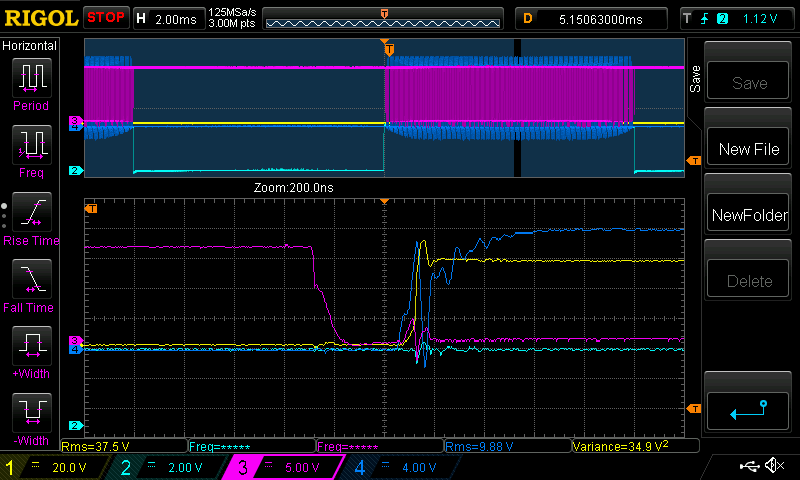 I could tune it further, to get a bit more damping. this is a large step in the right direction. I need to read your post Wiseguy next and this will take some time. wronger than a phone book full of wrong phone numbers |
||||
| wiseguy Guru Joined: 21/06/2018 Location: AustraliaPosts: 1296 |
After looking more carefully at all your CRO waveforms what I see looks identical to the ringing curse that usually occurs with paralleled FETs, and sometimes but less severely in a single FET. There is a feeling of deja vu to me. I spent hours trying every "cure" I could think of - similar to what you are doing. I found snubbers very ineffective for that HF ringing they may have modified or reduced it slightly but that was it. The only effective cure I found was putting a ferrite bead on the drain leg. Note with multiple FETs insulating pads must be used for each FET with a bead, they cannot share the same heatsink uninsulated despite all being at the "same" potential. All that does is short the beads out and they don't "bead" any more. It is also easily seen in some of your images that higher values of gate resistance can cause the lower FET to briefly commutate to on when the high side turns on. I agree that switching the FET more slowly does not seem to kick start the HF bursts of oscillation but has other negative effects. Maybe the slower switching helps to quench tendency to oscillate due to being in its slower & resistive switching region? With higher values of gate resistance the FETs do turn on (and off) more slowly, spending more time in their "linear" region, generating more losses - heat mainly. Lower values of gate resistance cause the FETs to switch more rapidly which also can tend to generate more radiated noise. I should add that my comments and results were all with my hardware so results might vary. I look forward to the next instalments  PS Your last post with image, the dark blue gate appears as classic gate "R" too high as it was commutated off whilst trying to turn on - due to miller I assume? The upwards blip of the yellow trace I interpret as some of the L energy being released back to the half bridge node during the momentary turn off. Edited 2026-02-17 11:49 by wiseguy If at first you dont succeed, I suggest you avoid sky diving.... Cheers Mike |
||||
| poida Guru Joined: 02/02/2017 Location: AustraliaPosts: 1476 |
yes, the dark Blue high side gate voltage trace seems very bad now. I put 4R7 gate resistors on the board for all 4 FETs since the smaller ones seemed to be a bit too fast. just to clear up one thing, no FETs are in parallel. Seeing the wild changes in high side gate voltage, I retested without the isolated probe, this time just a 10x probe, referenced to DC GND. I saw the same thing. Maybe I go back to 2R2 resistors, to help a bit with that high side gate voltage dip. I read your views on low side gate being turned on by capacitive coupling of low side drain going through fast dV/dt events. once low side gate gets this voltage, it has to be sunk via external parts. Interesting that HY4008 has an internal gate resistance! shorting the pin still means it's at best 3.2 Ohms. that will take some time to dissipate the charge created inside the chip. A follow-up on past question: yes I tested with one of your first completed 2 x 4 FET inverters. I thought that it was an interesting test due to your having SMD FET totem pole driver close to the FETs. This project is not intended for widespread use by others. I want a simple unit, maybe for the camper. I think we might find a solution that will be adequate and cheap and easy to build. But it is to be robust. At idle (no load) there is ZERO shoot through. this indicates to me it will survive. wronger than a phone book full of wrong phone numbers |
||||
| analog8484 Senior Member Joined: 11/11/2021 Location: United StatesPosts: 203 |
That's interesting. So, all the inverter boards with drain ferrite beads mounted like this effectively have not ferrite beads?  |
||||
| wiseguy Guru Joined: 21/06/2018 Location: AustraliaPosts: 1296 |
I don't have a clear view of the PCB tracks, but the drains usually have a PCB track connecting them together, so all of the Beads are effectively in parallel. When I did my testing with my PCB's the HF ringing was much worse than when the Drains were insulated from the heatsink. My testing was just a PCB & heatsink on the bench not built up in a chassis. The main issue is that the power/external connection to the Drains should be passing through the Ferrite Bead to get to the Drain, the bead provides a lossy high impedance to any tendency for HF oscillations to begin or establish in the first place. So in my experience and testing, power or Choke/toroidal connections to the heatsink should be avoided and FET drains should be insulated from the heatsinks. If at first you dont succeed, I suggest you avoid sky diving.... Cheers Mike |
||||
| poida Guru Joined: 02/02/2017 Location: AustraliaPosts: 1476 |
I was wondering if my voltage probe technique might be dodgy. In particular, the un-shielded 2 wires that connect the high side Gate and Source that then go into the isolated probe. my question was "is this voltage real?" I took 2 DC ground referenced DSO probes, put on on the high side Gate the other on the Source and used the DSO math function to subtract the Gate from the Source. good news for me is both probe techniques work well and agree with each other. But what is going on here? 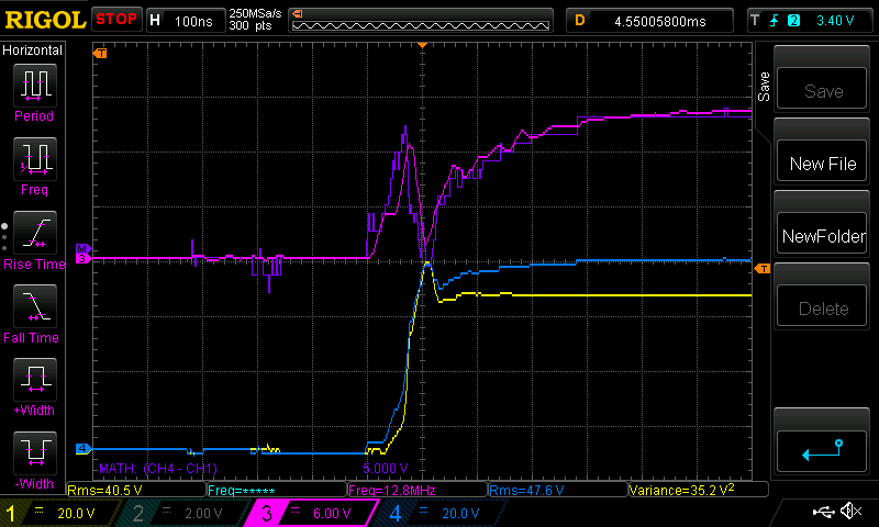 Yellow is high side Source or the output of the half bridge. This is the "zero point" for the high side FET Gate to work against to turn it on or off. Dark Blue is high side Gate. these are the 2 lower traces. Purple is the isolated differential probe and the very stepped dark Blue is high side gate minus high side source, i.e. what the gate is seeing and it should be the same as the isolated diff. probe output. there is maybe 10 ns delay for signals passing through the diff. probe and we can see this here. Yes, both Gate voltages agree. But after the high side FET is dragged up to DC supply, the gate voltage drops to near zero. This is very interesting. The near zero gate voltage (implying to me the FET is not conducting positive current FROM Drain to Source but is sort of open circuit) might explain why oscillations can be initiated and/or sustained. This test was when under 200 W AC load, when the high side FET switches on. I do not care too much what is happening to the low side FET, no doubt it has turned on during this curious time too, just to make it even more opaque for my understanding. wronger than a phone book full of wrong phone numbers |
||||
| analog8484 Senior Member Joined: 11/11/2021 Location: United StatesPosts: 203 |
Good point. I can't see how else they would be connected back to Vbat+. Given your findings, I wonder if this is why some inverters have large ferrite clips on Vbat+ (and Vbat-) connections in addition to the ferrite beads on the MOSFET drain pins. I have always thought those seemed redundant. |
||||
| analog8484 Senior Member Joined: 11/11/2021 Location: United StatesPosts: 203 |
Based on your previous scope capture: the high side gate dip looks like the result of low side false turn-on (~3.5V). I believe you took out the gate turn-off diodes for these scope captures. If so, I suggest putting them back in. |
||||
| Zathros Newbie Joined: 20/09/2024 Location: United StatesPosts: 7 |
I think what you are seeing here is the drain to gate capacitance of the upper mosfet working against the gate drive current during the mosfet turnon transistion. The gate voltage increases untill the mosfet starts turning on, then when the drain to source voltage is rapidly decreasing the gate drain to gate capacitance driven by the gate drive circuit is working as a very fast Miller Integrator. The gate voltage drops back down to the mosfet threshold voltage while the mosfet is running in linear mode. As soon as the mosfet is fully turned on, the gate voltage again rises to the voltage provided by the gate drive circuit. |
||||
| wiseguy Guru Joined: 21/06/2018 Location: AustraliaPosts: 1296 |
Sorry, I missed your reply. Usually the large ferrite devices clipped on input conductors are a last ditch attempt to help remove EMI from escaping the inverter box and thus onto the longer battery connect leads. These leads also act as an antenna. When inverters are designed/manufactured they are supposed to comply within specific values of conducted or radiated emissions. They are redundant to a point where the inverter will work fine without them but any radio within 20 metres may suddenly have whistles and buzzes etc added to what's left of the music. If at first you dont succeed, I suggest you avoid sky diving.... Cheers Mike |
||||
| The Back Shed's forum code is written, and hosted, in Australia. | © JAQ Software 2026 |
