Notice. New forum software under development. It's going to miss a few functions and look a bit ugly for a while, but I'm working on it full time now as the old forum was too unstable. Couple days, all good. If you notice any issues, please contact me.
Solar Mike Guru Joined: 08/02/2015 Location: New ZealandPosts: 1216
Posted: 09:48am 10 Feb 2026
Copy link to clipboard
Print this post
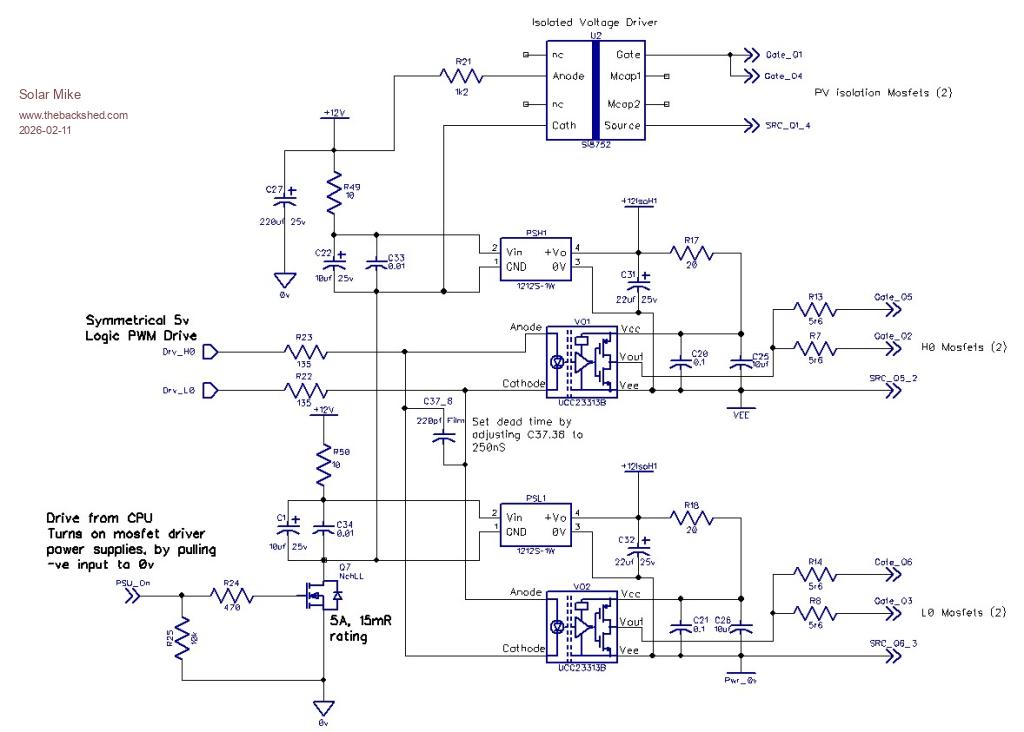
Thought I might have a go at making a MPPT Synchronous PV Charger using "E"-Opto mosfet drivers connected in an inter-lock arrangement. This allows the driver chips be mounted some distance apart and as close to the mosfets as possible. The interlock circuitry also sets the dead time between the H0-L0 devices, along with inputs for disabling the pwm if the cpu voltage rail drops for any reason and falling over to non-synchronous mode with low charge currents at very low duty cycles that would otherwise cause the buck circuit act as a boost driver, which tends to blow thing up. Usually I use dedicated 1/2 Bridge driver chips, these are not always optimal when driving multiple mosfets due to the long trace lengths required, so I thought this circuit would be interesting to play with.
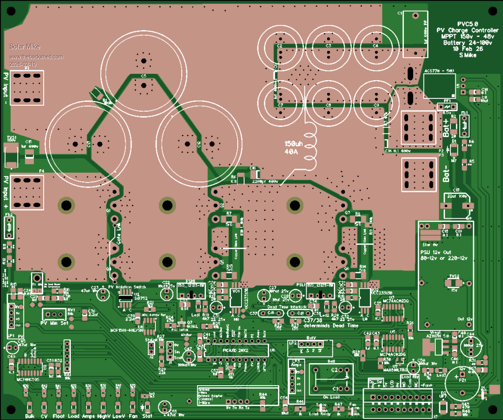
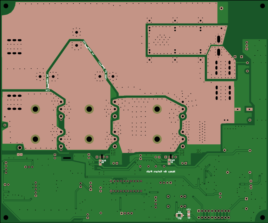
I will draw out the schematic, as some of it is a bit complicated, post bits of it here as I do so. The pcb is 204 x 170 mm 1oz copper, all high current areas are masked for tinning, this adds to the copper thickness and allows judicious soldering of extra copper wires to increase the current capacity, not sure what power this board will handle, should be ok at 40 amps, I now have a hand held thermal camera, so will be easy to pick out hot spots.
Here is the current layout:
Just noticed the bottom layer text is reversed, will fix that, a tick box has unchecked itself.
Cheers Mike
Solar Mike Guru Joined: 08/02/2015 Location: New ZealandPosts: 1216
Posted: 08:36pm 10 Feb 2026
Copy link to clipboard
Print this post
Schematic showing the mosfet interlocked drivers and isolated bias supplies, I haven't drawn in the mosfets nor the main power electrolytics, buck choke etc.
Edited, updated schematic changes. Mike Edited 2026-02-11 19:04 by Solar Mike
Solar Mike Guru Joined: 08/02/2015 Location: New ZealandPosts: 1216
Posted: 09:27am 11 Feb 2026
Copy link to clipboard
Print this post
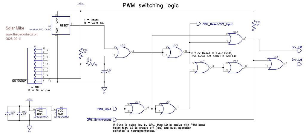
Here is the schematic for the PWM control logic, I wanted to use logic gates that had an invert function and could output +-24 mA drive. The "E"-Mosfet driver inputs require approx 10mA and this is just outside of allowed safe values for normal cmos gates. Having a bunch of MC74AC02 quad Nor gate chips on hand, decided to use them.
Either user switch = off or the MAX810L detecting a low cpu voltage, will raise a fault flag, that turns off the PWM drive and also inputs to the cpu so it can shut down properly; Pic chips pwm output goes haywire when the supply rail fails, prob same for most cpu's, could be a reason why some users have inverters that occasionally self destruct.
At low charge or duty cycles the cpu can switch the drive to Non-Synchronous mode, preventing the buck circuit acting as a reverse voltage booster.
Think that's about it for now, will send the gerbers off, may take awhile as Chinese are on holidays; will report back once I have something running.