
|
|
Forum Index : Electronics : Another three-stack toroidal transformer
| Author | Message | ||||
| analog8484 Senior Member Joined: 11/11/2021 Location: United StatesPosts: 203 |
It would be interesting to know what the ripple voltage (peak to peak) was under very high current. I couldn't find 80x30mm KEMET cap but found 82x36mm (https://www.digikey.com/en/products/detail/kemet/ALS30A103DE063/4833245). Assuming that's the one, the 100Hz ripple current limit is 10.8A and ESR is 17mOhms. That's probably good for 10-20C rise at the ripple current limit. So 8kW with 6 caps total with no noticeable heat suggests the 100Hz ripple current is well below the ripple current limit in the 8kW (~160-200Adc) load range. So, guesstimating the ripple current is < 25% of limit (2.7A/cap) or 16.2A total. The means the ripple current is ~10% of the load current. That seems like an optimal target for design. That seems a practical design target given the cost of the caps. |
||||
| analog8484 Senior Member Joined: 11/11/2021 Location: United StatesPosts: 203 |
I wonder about this too because some inverters have monitoring for ripple voltage and provide the option to shutdown if it's too high (e.g. 5Vrms). The concerns for high ripple voltage include the wear from micro discharging/charging cycles, decreased charging efficiency when charging and impact on loads. IIRC, the ideal ripple voltage is ~1.5Vrms under rated load for 48V systems. Not sure how practical that is in practice. Edited 2025-04-21 04:41 by analog8484 |
||||
| KeepIS Guru Joined: 13/10/2014 Location: AustraliaPosts: 2177 |
There seems to be some confusion between the Current drawn by this Inverter from a Battery and the residue from a filter designed to remove particular frequency components from an output. To see 20kHz Inverter noise / ripple and step wave HF/Uhf Inverter switching Noise on the DC bus you would typically use a DSO. An Isolated Hall sensor with signal processing aims to remove interference noise and accurately measure the DC current flowing through a cable into the Inverter. The Hall Sensor on the DC bus feeding a pure sinewave Inverter will be outputting a 100HZ positive going voltage, proportional to the Current flowing along the cable into the Inverter. The positive Hall Sensor voltage looks, sort of, like the sinewave the Inverter is generating with this current flow. Any readings with an AC clamp meter on the DC cable will be just a meaningless indication that there is indeed 100Hz current flowing. 100hz DC Inverter Input current and associated voltage variation is not ripple in the true sense, more like load regulation of the DC Bus, you can't effectively filter everything from the Cable between the Battery and the Inverter FETS, especially at very high currents. The current can be, in my case, 700A Peak @ 100Hz for the duration of large Induction motor or Brushed motor starting Load, but it is always there if the Inverter is Powered, measured in mV (sensor out) if the Inverter is at Idle. The DC Voltage deviation will primarily be a function of Battery bank capacity and Power Stage Capacitor values (quality). Systems drawing high sustained currents generally have larger Battery capacity and lower voltage variations with current, especial right at the Battery terminals. You mention 5kW to 6kW, I would think that good quality correctly sized Filter caps and a suitably sized Battery bank would reduce any voltage variations to a small value. The HAll Sensor output voltage monitored by a DSO has been posted numerous times for both low currents and extremely high currents, obviously this is not the voltage variation on the DC supply rail. An Inverter doing what it's supposed do is not the really definition of Microcharging a battery, maybe Micro cycling. However there are no definitive results on Microcharging below 100% SOC, even at full SOC which a LiFePO4 should NOT be sitting at for any length of time, normally one would have the Solar charging/BMS setup correctly to reduce microcharging near 100% SOC. Micro cycling concerns are being tested but are not showing and real world definitive results AFAIKT. EDIT: There is 183mV RMS halfway between the Batteries and the Inverter on the DC bus with a 3kW Load, peak 100Hz current is sitting around 160A. Across the Battery it is <20mV with some of that being 20KHz Inverter switching and other HF noise being induced into Measurement setup and balanced leads. FYI There is 80mv induced into the very short twisted Differential Probe leads with the Prob leads disconnected and sitting 200mm from the Solar Chargers and top Battery bank. It is at 3kW and would be 6kW, I might measure it one day at 12kW  Do you know over what frequency range was that suggested specification? Do you know over what frequency range was that suggested specification? . Edited 2025-04-21 12:03 by KeepIS NANO:Inverter V 8.2ks - Linux AvrDude GUI script V4.1 |
||||
| FET cemetery Regular Member Joined: 17/04/2024 Location: AustraliaPosts: 74 |
I was more concerned by the 100Hz seen by the battery. I'm pretty sure the large current swings I was worried about are just measurement artifacts, and this is confirmed by the lack of significant battery temperature change when the car is charging. More progress 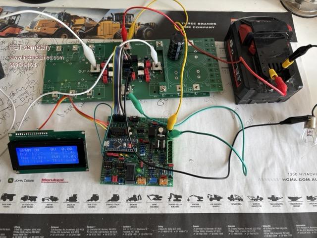 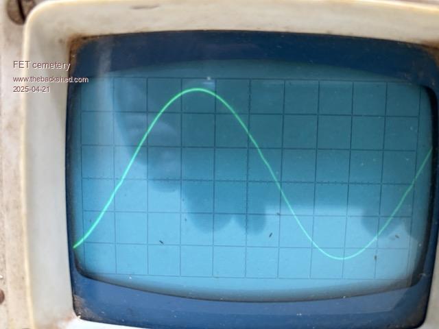 4 fets, running unloaded No stone unturned, no FET unburned. |
||||
| FET cemetery Regular Member Joined: 17/04/2024 Location: AustraliaPosts: 74 |
Going for the drilled and tapped flush mount heatsink 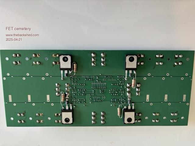 No stone unturned, no FET unburned. |
||||
Revlac Guru Joined: 31/12/2016 Location: AustraliaPosts: 1277 |
Your Build is going well.  The aluminium bar under the mosfets would be preferred, give a little more clearance for the gecko's, I just chased one out of my inverter.  Cheers Aaron Off The Grid |
||||
| FET cemetery Regular Member Joined: 17/04/2024 Location: AustraliaPosts: 74 |
The aluminium bar might let the mice in though. 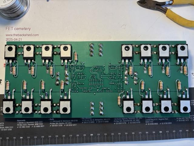 The fet board really is a work of art, shame it has to be hidden by the heatsink. No stone unturned, no FET unburned. |
||||
| FET cemetery Regular Member Joined: 17/04/2024 Location: AustraliaPosts: 74 |
Is it better thermally to have the heatsink further from the pcb with the aluminium bars? I'm planning on having heatsink fans come on sooner rather than later. No stone unturned, no FET unburned. |
||||
| wiseguy Guru Joined: 21/06/2018 Location: AustraliaPosts: 1296 |
Conjures up an image of a mouse doing the limbo - would need a real runt though.... Hopefully the enclosure wont have any openings large enough to let mice or lizards or moths in. Its not so much them but also their urine and other excrements that might corrode and/or conduct. I still reckon there is some trick photography there, how did you get the bead on the FET and back into the Drain hole in the B+ plane? Ok took another look I think my beads were 5mm long, my calibrated? eyes think yours might only be about 4mm long? Who would have thought a 1mm would make so much difference, I always said length isn't everything.... The proximity of the FETs/heatsink to the PCB is irrelevant should make no difference the FETs seem to run a few degrees above ambient, even the heatsink fins are basically redundant. Just a note about the beads, ferrite can conduct so don't let the beads on the low side centre Drain leg touch the B- plane maybe bend the Drain leg slightly to have at least 0.3mm clearance to the ground plane or a layer of Kapton tape under the bead. I once ran active traces under an RM8 core that rested on the PCB the results weren't pretty, I was told somewhere that ferrite is an insulator - not always ! A small piece of Mylar under the core sorted that out until the next revision. Neat job on the power board! Edited 2025-04-21 23:39 by wiseguy If at first you dont succeed, I suggest you avoid sky diving.... Cheers Mike |
||||
| analog8484 Senior Member Joined: 11/11/2021 Location: United StatesPosts: 203 |
Nice. I think you have the most over-engineered DIY inverter system ever The recommendation is about the low frequency ripples at 100Hz or 120Hz. Edited 2025-04-22 03:32 by analog8484 |
||||
| FET cemetery Regular Member Joined: 17/04/2024 Location: AustraliaPosts: 74 |
Wiseguy - the beads I used (from an ebay link on either yours or KeepIS's threads late last year) are 4.1mm long, 3.55mm dia. I'm sure that's a nice round number in inches. I was going to leave them off the +ve fets until I realised how easily they would fit, only downside is that you can't get a soldering iron to the drains on the underside of the board. 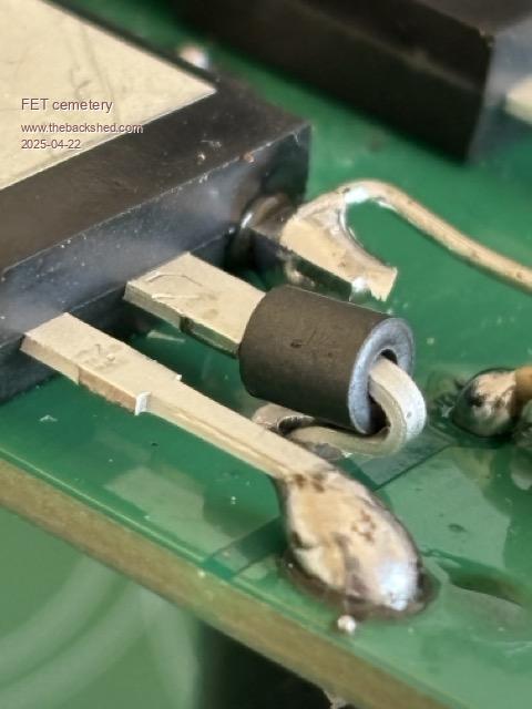 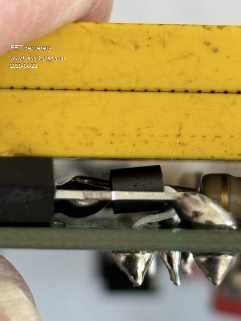 The -ve drains have enough clearance I think, might just apply a dab of glue or some tape to stop them rattling around. 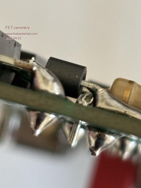 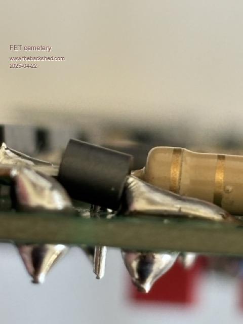 No stone unturned, no FET unburned. |
||||
| FET cemetery Regular Member Joined: 17/04/2024 Location: AustraliaPosts: 74 |
A couple of things that I noticed assembling the power boards: With any of the components soldered to the big +ve, -ve and output copper planes you have to allow plenty of time for the copper to heat up or the solder won't flow cleanly. I was worried about heat damage to some components, particularly the zeners, but all was good. Soldering the battery, output and capacitor terminals takes a lot of heat, I used an 80W iron with no temperature control and would consider that to be the bare minimum necessary. The only mechanical support where the gate resistors are soldered to the fet gates is the solder, ie they're not twisted around the gates or anything (at least not the way I've done it) they're just resting there before being soldered. Based on what I've heard from a friend who repairs valve radios I would only use a lead based solder here, apparently lead free solder tends to be quite brittle when there's mechanical strain on a joint and prone to failure within a couple of years. No stone unturned, no FET unburned. |
||||
| FET cemetery Regular Member Joined: 17/04/2024 Location: AustraliaPosts: 74 |
Oh yeah, and the little transistors, Q17 to Q24, are really small and fiddly to get in. Next time around I will solder them in BEFORE the capacitors! No stone unturned, no FET unburned. |
||||
| wiseguy Guru Joined: 21/06/2018 Location: AustraliaPosts: 1296 |
Thanks for the close up pictures, all nice rounded Drain legs no sharp 90 degrees - well done. With regard to the soldering access on the drain bead side I solder them with a normal Hakko hand soldering iron but the solder rarely tracks through to the other side. Now I apply an ample amount of solder to the solder side and afterwards I use a Hakko hand held solder sucker onto the drain leg and as it reaches the PCB and melts the solder move it up and down a few mm on the leg and then remove. The solder then is coaxed to track fully through to the other side of the PCB as if by magic, the whole process takes ~ a few seconds. Maybe a high wattage iron would achieve similar results but if you have access to a solder sucker it works a treat for this purpose. Not sure of your reason for not using an aluminium bar and I'm not not criticising as you no doubt have a good reason, but if a tap jams or breaks off in the heatsink it is a real problem. If you use 6mm x 25mm bar or 10 x 25, It allows bench testing at relatively high power for short periods and the module removal from a heatsink takes just a few minutes. There is plenty of room for gate resistors and drain clearances etc but granted the whole assembly is a bit taller. Also use of countersunk holes and screws on the aluminium bar to heatsink interface, with the nuts available on the PCB topside means no tapping is required. If at first you dont succeed, I suggest you avoid sky diving.... Cheers Mike |
||||
| Murphy's friend Guru Joined: 04/10/2019 Location: AustraliaPosts: 678 |
Wiseguy's PCB's are usually very good but I think he had a senior moment when designing the ferrite bead location .All that was required is to place a 3mm thick board (anything non conducting and capable of taking a little heat) at the *back* of the mosfet, between it and the PCB. The mosfet leg PCB holes could then be in a straight line (not staggered) if the legs were bent at 90 deg where they reduce in width. Congrats on making a tricky soldering job doable  . . |
||||
| Revlac Guru Joined: 31/12/2016 Location: AustraliaPosts: 1277 |
I found it a bit of a task (at first) for the 60w soldering iron to solder the large terminals and capacitor boards, I had another 30w soldering iron close by, just dab that on just after most of the work is done by the 60w and it all went well and easy, seems to be a few different ways to achieve a good result.  I did hold the controller board up to the light and could see light get past one of the resistors or something, soldered that up, fixed. Cheers Aaron Off The Grid |
||||
| wiseguy Guru Joined: 21/06/2018 Location: AustraliaPosts: 1296 |
I've had lots of senior moments but it's not relevant here. I did not design a ferrite bead location I wasnt going to use them there. Due to the small improvements with the beads on my Rev1 boards I was going to dispense with them for the high side FETs on Rev2. But when building Rev2 I changed my mind and included any improvement gains. I also don't feel like spending another huge amount of time redoing the artwork for this minor issue when it already performs just fine. To get the lowest impedance (widest) ground planes for high current is what led to the staggered pins including cutting off the gate pin. Having the pins in line degrades this aim. However I would like to explore your PCB spacer suggestion which may have merit. Constructive criticism and improvement suggestions are always most welcome & encouraged. Edited 2025-04-22 21:16 by wiseguy If at first you dont succeed, I suggest you avoid sky diving.... Cheers Mike |
||||
| Murphy's friend Guru Joined: 04/10/2019 Location: AustraliaPosts: 678 |
I am guilty of having copied a lot of your ideas with regard to electronics (and those work very well) but having designed PCB's for a living many years ago it does seem to bug me seeing their assembly made more difficult than it could be. I know the ferrite bead was an afterthought, it's just your fitting of it. Spacing that mosfet up from the PCB lets you bend the drain pin at 90 deg (rounded bend if you think it makes a difference) and easily fit that bead on it. The staggered pins can easily be avoided by soldering the tail of a solder lug onto the short path to the ground plane. My power boards have them beside having identical polarity power planes on top *and* bottom of the PCB. That way I can use 1oz boards, even for the 6KW inverter since the tracks combined make 2 oz copper with twice the surface area. Never had any PCB track problems with my 6KW inverter, using just 12 HY5608's. |
||||
| FET cemetery Regular Member Joined: 17/04/2024 Location: AustraliaPosts: 74 |
I'm not entirely sure why I'm not using an aluminium bar myself to be honest! I think the end result will be tidier and simpler with the flush mount heatsink, certainly a bit more compact. I'm leaning towards putting everything bar the big transformer in one of the old SB1700 GTI cases in which case space will be a bit limited. Thread tapping is something I quite enjoy in small doses, there's an almost meditative level of relaxed concentration required. Same with assembling the boards, particularly the power board, once I got in to the rhythm of it. I might revisit the drain soldering, I think it might be possible with a sharp tip on the iron. No stone unturned, no FET unburned. |
||||
| KeepIS Guru Joined: 13/10/2014 Location: AustraliaPosts: 2177 |
I have thread tapped two inverters, then I tried wiseguys idea, as much as Klaus loves basket weaving and tapping holes wiseguys idea was sooooo much quicker with no chance of breaking a tap, my brain meditates without telling me these days, or is that OLD-timers disease.wiseguys boards do have wide power planes on both sides, I've run a single board at over 8kW, they were warm but not overly so, I believe Mike (wiseguy) suggests around 6kW for the boards, I could be wrong though? NANO:Inverter V 8.2ks - Linux AvrDude GUI script V4.1 |
||||
| The Back Shed's forum code is written, and hosted, in Australia. | © JAQ Software 2026 |
