
|
|
Forum Index : Electronics : Another three-stack toroidal transformer
| Author | Message | ||||
| FET cemetery Regular Member Joined: 17/04/2024 Location: AustraliaPosts: 74 |
Hmm kind of committed now, the heatsink is marked and I've started drilling. Will change my mind if it gets messy! Soldering the drains is possible, just not pretty. 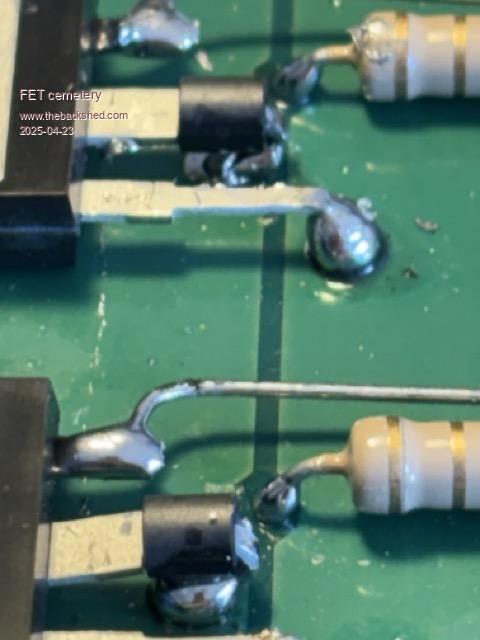 No stone unturned, no FET unburned. |
||||
| Murphy's friend Guru Joined: 04/10/2019 Location: AustraliaPosts: 678 |
OK, it's possible that I too have the old-timers disease since I cannot locate wiseguys incredible tapping method in his long post. Any clue where this info lurks now, it's just possible I missed one of the better ideas wiseguy had  . .Yes, I do like manual tapping but have not yet tried basket weaving. Any suggestions how I start with that or do I have to join the basket weaver union first  |
||||
| KeepIS Guru Joined: 13/10/2014 Location: AustraliaPosts: 2177 |
I think basket weaving caused my old-timers, but like everything else these days, I don't quite remember what came first  I remember (shocks of disbelief) that the three of us had a discussion about his scandalous suggestion at the time. It involves drilling a small hole through the aluminum bar, then a slightly larger hole on the other side of the heat bar deep enough for a screw reach and then drive a small nut into the hole. Or with a long screw that fits through the heat bar, pull the nut into the hole - this from fading memory, it my trigger an I remember moment, again use all info with caution, I may have dreamed it all NANO:Inverter V 8.2ks - Linux AvrDude GUI script V4.1 |
||||
| Godoh Guru Joined: 26/09/2020 Location: AustraliaPosts: 667 |
I used to call Electric motor rewinding "glorified basket weaving" Transformer winding is not much different, winding torroids from scratch is not a lot different, but motor winding takes it all to a different level. Pete |
||||
| Murphy's friend Guru Joined: 04/10/2019 Location: AustraliaPosts: 678 |
Thanks for the refresher course, it looks like this method was not up to my standards and hence not worth remembering .I suppose it might work with short heatsink fins... But since the hole *has* to be located very accurately to line up precisely with the PCB hole this method looks dodgy to engage the mosfet mounting screw squarely with the nut pressed in at the far side of the heat sink. I'm surprised you credit wiseguy with that, thought he was working to a better standard .A refresher of the 'Klaus' method (requires a pedestal drill): mark and center punch the holes as accurately as possible. Marking could be done through the PCB holes if it is clamped firmly and precisely at the correct location. Tip: the holes should fall into the valleys between the fins - I design my PCB's to do that. drill 2mm holes *carefully*, with plenty lubrication, at the center punch. enlarge the holes to 2.5mm tap the holes M3 using a long taper tap or numbered taps (1-3). |
||||
| KeepIS Guru Joined: 13/10/2014 Location: AustraliaPosts: 2177 |
This is for the heat transfer bars some of us use between the FETS and the Heatsink There are no fins on aluminum heat transfer bars, imagine something flat on both sides The hole alignment is easy and the nut is secured perfectly as it bites into the walls of the larger hole and never moves, no mater how many times you remove the PCB. It's No more dodgy then the pilot holes you drill in the aluminum bars if you tap them. Yes we also use a pedestal drill and the method description assumes one knows how to get a nut to go perfectly square down the hole.  Edited 2025-04-23 19:07 by KeepIS NANO:Inverter V 8.2ks - Linux AvrDude GUI script V4.1 |
||||
| wiseguy Guru Joined: 21/06/2018 Location: AustraliaPosts: 1296 |
Klaus sometimes you seem to come on here a bit snarky, curiously my daughter also gets like that each month...I know its your idea of sport or fun but we seem to all get on just fine without having to stir the pot resorting to chucking barbs at each other. My latest method of FET mounting to the heatsink was posted over a year ago, my current method is here: 2024-06-04_174543_FET to Heatsink Mount.pdf I did also pioneer the method that KeepIS is using and it does work perfectly, when the nut seats at the bottom of the part drilled hole it is perfectly square to the central M3 clearance hole which I usually drill to 3.5mm. The nut can be pushed in using the pedestal drill from the rear or pulled in with a high tensile hex 3mm screw, both methods work fine. Maybe approaching the task with a positive attitude also helps with the success of the task at hand? The latest method is even easier especially if you have a proper countersink bit. The major difference is that the nut is the fastener from the topside. So how tight to do up the screw or nut for compressing the FET/bar/heatsink interface, glad you asked. For ~ 25 years I have used the following method. I keep the spring washer visible and tighten until the split in the spring washer looks like a normal washer ie pulls just flat, this corresponds to the driver becoming stiff, I take it a bit further maybe 10 - 20 degrees rotation, voila job done! It does not squeeze the bejesus out of the silicon pads nor allow the tension to ever become loose. However I never use a square washer for this job I always use the wider flat spring washer such as these M3 3933411.pdf the obscured thickness dimension is 0.8mm. But note this is an Element14 part and they only seem to stock the stainless steel version - they may be fine - I have only ever used the steel/zinc type. By the way I have clamped the PCB to the aluminium bar and using a TO220 bush in the PCB's FET hole to avoid PCB damage, I lightly drill each hole about 1mm deep and then remove the PCB and continue drilling the hole starts to full depth which gives excellent registration of PCB hole centres to the bar. Edited 2025-04-23 21:02 by wiseguy If at first you dont succeed, I suggest you avoid sky diving.... Cheers Mike |
||||
| wiseguy Guru Joined: 21/06/2018 Location: AustraliaPosts: 1296 |
Apologies to FET Cemetery for polluting his thread with all this stuff. By the way my colleague (when I was ~17) used to refer to complementary cemetery instead of symmetry. His rationale was that if something failed with all the direct coupling it resembled a cemetery of dead semiconductors  Not too dissimilar to your handle. Not too dissimilar to your handle.If at first you dont succeed, I suggest you avoid sky diving.... Cheers Mike |
||||
| KeepIS Guru Joined: 13/10/2014 Location: AustraliaPosts: 2177 |
Even Better NANO:Inverter V 8.2ks - Linux AvrDude GUI script V4.1 |
||||
| wiseguy Guru Joined: 21/06/2018 Location: AustraliaPosts: 1296 |
FYI Whether you are an ex PCB designer or just back shedders there are standards and application notes that describe the correct way to create bends on high current legs to avoid longer term breakdowns and failures, especially with repeated heating and cooling. AN-1031.pdf If at first you dont succeed, I suggest you avoid sky diving.... Cheers Mike |
||||
| FET cemetery Regular Member Joined: 17/04/2024 Location: AustraliaPosts: 74 |
OK, I've recovered from the transcendent meditative bliss of drilling and thread tapping, went pretty well really, only broke one drill bit early in the piece. My drill press won't hold a 2.5 mm bit so I tried drilling with the cordless drill. Murphy's friend is right, a drill press is necessary for this, got a drill bit with a hex bit on the end (meant for an impact driver) and used that in the drill press and no further problems. Slow and steady wins the race here. Tapping just needs patience and a bit of light oil. A small tap holder so you can feel what's going on helps. I used a tapered tap, 1 1/2 turns in then 1 turn back and take it all the way out and clean it as soon as you feel it tighten up. 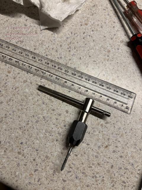 The way my heatsinks were originally drilled meant there was no way of having all the fets clear of the existing holes. To fix this I put some thermal paste on a screw, tightened it firmly into the hole and cut it off with a dremel. Ground it down just below the level of the heatsink and filled the gap with some thermal paste before sticking on the insulating thermal mat. 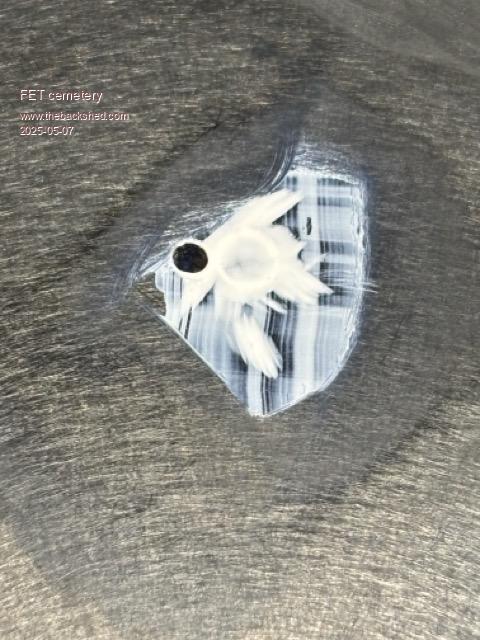 The finished product 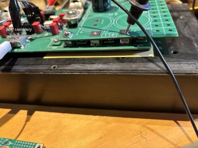 No stone unturned, no FET unburned. |
||||
| FET cemetery Regular Member Joined: 17/04/2024 Location: AustraliaPosts: 74 |
Started testing today using the big transformer and something is clearly not right. I don't have a proper current limited power supply so I've been using 18V cordless drill batteries with an automotive tail light globe in series as a current limiter. At 18V unloaded all seems well, a good enough sine wave on the scope and about 600mA idle current. At 36V the transformer has a noticeable hum and the sine wave is starting to look a bit gnarly. At 54V the pwm is down to about 70% but the hum is still there and the sine wave is not great: 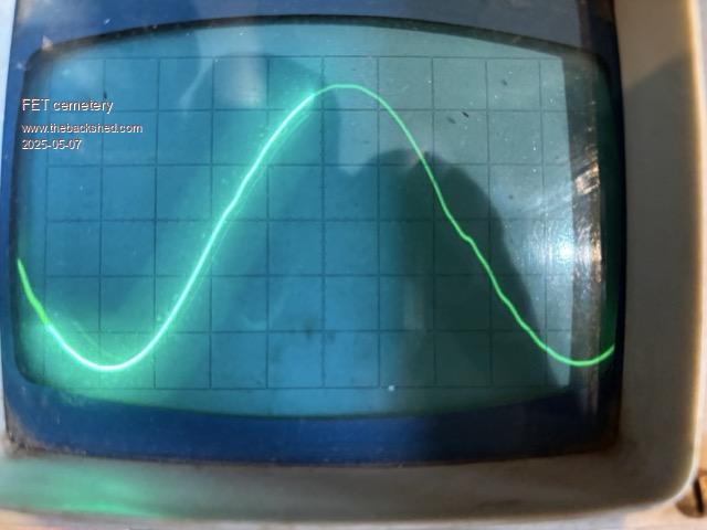 This was all with 2x 470uF capacitors on the power board, the 2 chokes with 4 turns through 8 sendust rings each and 4.7uF across the transformer output. Thinking this could be due to the temporary wiring to the boards and the ancient 470uF caps, I put a 5600uF cap on the power board. Got about 2 seconds in to the slow start at 18V and pulled the power, horrible noise from the transformer and the waveform (out of the corner of my eye, not really looking at it) was all over the place. Any ideas? I haven't checked anything yet except to confirm the same behaviour with both my nano boards (didn't try the 5600uF on the second one!). Probably won't get a chance till the weekend. Idle power at 54V was 35W. Nothing was running even remotely warm, no magic smoke. No stone unturned, no FET unburned. |
||||
| FET cemetery Regular Member Joined: 17/04/2024 Location: AustraliaPosts: 74 |
I'm thinking it has to be one of the bias supplies or something downstream of them. Wondering if I didn't cook one of the low side Zeners when I soldered them in. Fets all check out ok with the meter, drain - source resistance 1M9 and a bit. No stone unturned, no FET unburned. |
||||
| phil99 Guru Joined: 11/02/2018 Location: AustraliaPosts: 3293 |
The drive to the primary needs to have perfect symmetry. Any difference between the half cycles produces a DC component**. Your primary circuit DC resistance may be just a few milliohms so even a small DC voltage can produce a large DC current pushing one half-cycle toward saturation, which increases the current on that half cycle even higher. This positive feedback can result in full saturation. Magnetic amplifiers and saturable reactors work on this principle. A DC ammeter in series with the primary will show if this is the problem. ** All the components of a waveform can be calculated separately and combined at the end. |
||||
| FET cemetery Regular Member Joined: 17/04/2024 Location: AustraliaPosts: 74 |
Thanks Phil will check it. No stone unturned, no FET unburned. |
||||
| wiseguy Guru Joined: 21/06/2018 Location: AustraliaPosts: 1296 |
Idle power appears quite high. What was the secondary voltage at the 54V & 35W input? I do understand your series light globe, but probably a better method is to use a fuse holder and 2A, 5A, 10A, 20A fuses as appropriate as testing progresses. Keep in mind that the 4 x FETs combined have around 1,000A capability, yes I know the DC caps can supply large momentary destructive high currents. What is the idling current at 54V and no choke/transformer connected? I need some ball park figures to try to get a better handle on whats happening. If at first you dont succeed, I suggest you avoid sky diving.... Cheers Mike |
||||
| FET cemetery Regular Member Joined: 17/04/2024 Location: AustraliaPosts: 74 |
Secondary voltage at 54V & 35W was 240V. Will get back to you on no choke / transformer current. Thanks. No stone unturned, no FET unburned. |
||||
| FET cemetery Regular Member Joined: 17/04/2024 Location: AustraliaPosts: 74 |
"Idle power appears quite high." Yep, the transformer was humming loudly enough to be annoying in a quiet-ish room. I'd imagine 40+ kg of transformer is a pretty inefficient loudspeaker, could easily see 5 or 10W being dissipated there. Could feel it vibrating when I touched it. Just so we're all on the same page the power board is WG30-Rev2 and the nano board is WG39-Rev7. With nothing connected to the output it draws .128A at 53.3V, a touch under 7W. R4 has -2.7V across it measured from B-, D5 has +12.2V. The high side supplies are ok too, 12.43V across pin 5 and pin 8 of OC1, 12.50V for OC2. C10 is listed as Tantalum or Al on the circuit diagram but not the BOM I was using, I've missed that and used a 10uF electrolytic. Could this be causing problems? The 5600uF capacitor was tried at 36V not the 18V I originally said. At the higher voltages I was using an automotive headlight globe to limit current. With 2 x 470uF the globe was cold, adding the 5600uF (and not changing anything else) sent the current way up, the globe was properly glowing when I cut the power. I would estimate a good 3 or 4 Amps plus. The nano board was in test mode with only AC voltage feedback connected. Just because changing nano boards makes no difference doesn't mean they're off the hook, they were both assembled together and it's not beyond me to make a stupid systematic error. Lastly, I know I haven't followed Wiseguy's test procedure to the letter but starting with low voltages and small capacitors has no doubt saved me from living up to my username again! No stone unturned, no FET unburned. |
||||
| FET cemetery Regular Member Joined: 17/04/2024 Location: AustraliaPosts: 74 |
Could it be dodgy nanos? The Atmel logo looks a bit suss. 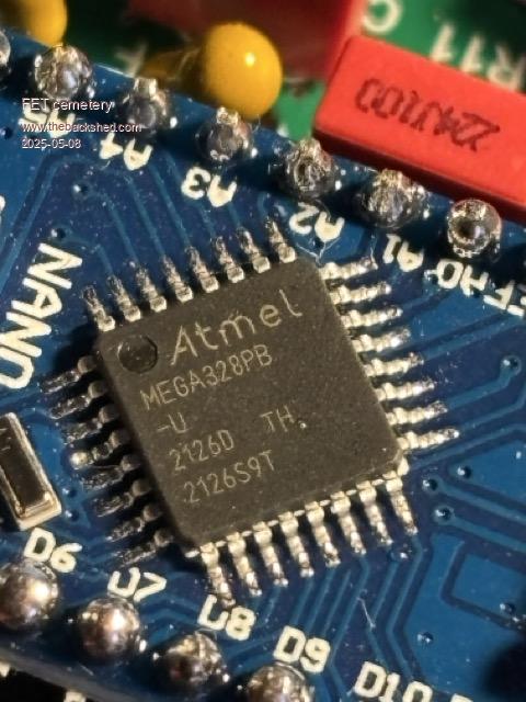 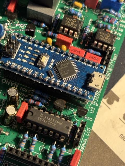 No stone unturned, no FET unburned. |
||||
Revlac Guru Joined: 31/12/2016 Location: AustraliaPosts: 1277 |
I had the exact same nano's with the micro usb, they run fine in the inverter , I just had issues with the USB on the old computer, So I ended up using them for running the LCD, you can try other Nano's if you have some, But I think something else is a bit off, will have a look later. I have also an Electrolytic for C10. Edit 2 I think you need to do some testing from the beginning, checking power consumption as certain parts are plugged in and or cables connected etc, Mike sent me a list on which ones to do in the correct order, just cant find it at the moment. I have the results but it would not be relevant to post it here. Edited 2025-05-08 17:58 by Revlac Cheers Aaron Off The Grid |
||||
| The Back Shed's forum code is written, and hosted, in Australia. | © JAQ Software 2026 |
