Menu
JAQForum Ver 19.10.27

Forum Index : Electronics : Inverter building using Wiseguys Power board and the Nano drive board

   Page 30 of 30    
Posted: 12:06pm
22 Mar 2026
Copy link to clipboard
nickskethisniks
Guru

Thanks! Btw, I'm really impresssed with the outcome so far! With just 1 switch it comes a live.
Edited 2026-03-23 08:29 by nickskethisniks
 
Posted: 02:36am
23 Mar 2026
Copy link to clipboard
Revlac
Guru


Yeah just love the way it works.  
 
Posted: 05:34am
25 Mar 2026
Copy link to clipboard
KeepIS
Guru


Note: This is not a alternative to the wiseguy initial setup and test procedure for newly assembled Inverter boards.

When building the WG Inverter, or after any mods etc, once the controller board has passed it's pre-flight tests and the power board isolated supplies and wave forms have been checked, or after changing anything or making Inverter modifications:

My final pre-launch check is made with a small 1k resistor connected between a 14Vdc supply and power board B+ T1. Terminal T2 is common, The power supply supply current trip is set to 300ma and voltage set to 14Vdc.

With no power applied, the controller in Test mode, and a small value CAP board fully discharged, the power board is connected to the toroid, a CRO or DSO is connected across the AC output of the toroid, any low cost small DSO will do.

The basic power board, isolated supplies and SPWM drive and FETS, along with any obvious Toroid faults/errors shorts and AC output filter and wiring errors can have a final check here.

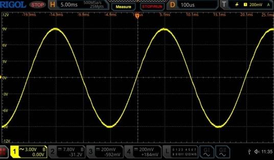
With 14v applied to the controller, total current draw should be Less than 270mA for around 16vac P-P sine wave output, it depends on your turns ratio and toroid design voltage, do not place any load on the output.

NOTE: You will need to temporarily adjust the "Nano Menu" Item 2 "Capacitor Calibrate" voltage above Item 1 (Battery DC calibrate voltage), as the supply voltage to the FETS is via a 1K resistor, I normally enter 50V in Item 2 to stop the AC sine wave rising and falling, you do this with the test setup running.

The AC output will be rising and falling as PWM ramps up and down due to the small cap bank, which is unable hold the voltage constant as AC starts to generate, the voltage drops quickly across the FETS, the Nano detects this and ramps PWM down, rinse and repeat, this will not hurt anything. Once Item 2 is set high enough, the AC output will hold still.         

There are no really high value caps or high DC voltages to destroy things, so if you missed something in the test setup, and you have set the power supply correctly, the maximum current should be limited to around 300mA, just a few watts, and whatever a very physically small sized cap can supply from 14V, which is also very little.

Do not go above 14V for this test.

NOTE: The test cap boards combined total capacitance must be NO more than a small size 1000uf 47v cap, small = less than 20mm high and 15mm across, this is important as these normally have a poor/high ESR.

If you made a mistake with FET mounting, or have any shorts or incorrect SPWM drive, the current will increase and voltage will drop and-or the AC output will fall way below 16vP-P.

Obviously you won't get this waveform and AC voltage if the SPWM drive connections are wrong, or there are shorts on the board, or there is a Toroid or wiring problem.

The AC output should look like the following, an AC output filter is not connected in this bench test setup, the DSO probe is connected across a 3uf to 4uf 400vac SPWM filter CAP which should be wired permanently across the secondary of the Toriod, the secondary being the AC output.


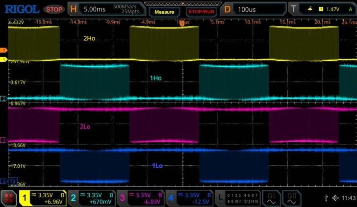
FYI Below: The Controller SPWM HI-LO output switching on J5, referenced to common (GND)

A test plug with flying leads is simple to make to plug into J5, solder short leads to pins 1 to 4, these connect to the DSO probe/s, in my case the 4 channels of the DSO are connected to these pins.

Solder a short ground lead to Pin 8 of J5 for the DSO probe earth clips.

Finally a 1k resistor will need to be connected between pin 5 of J5 and the DC input if you are using my Code.

Pin 7 of J5 has +12v on it, it's not used here and should be cover with heat shrink tube.

Make sure all pins on the plug are covered with heat shrink, especially Pins 5, 6 and 7.

Obviously the Controller board is not connected to the Power board:

Controller board setup:  

The LCD is connected.

     DC input: 12V
Current limit: 100ma

When running:

Current draw:  82ma
       Power: 986mW


EDITED: Added missing info.
Edited 2026-03-30 08:53 by KeepIS
 
Posted: 12:39am
01 Apr 2026
Copy link to clipboard
KeepIS
Guru


Since this is a dual Inverter build, I wanted to include the small external Over Current trip circuits I made, hopefully this time making more sense than my first attempt some time ago in the thread.

I wanted to clarify my use of three AC current sensors a little more, along with the DC peak meters and Peak DC input over current trip. It may look like I'm complicating the build, but in reality it's turned to be the opposite in a Dual power stage Dual Toroid build.

NOTE: No modifications are needed to the Nano Code:

The Dual Inverter design can switch between a powerful single stage lower "idle power" Inverter and a two stage Very High power Inverter, with only 23 watts extra idle power in my case. My Inverter does NOT incorporate dual stage switching, it is hard wired as a 12kW Inverter with a Peak DC input of 48kW.

I have a separate current trip circuit for each power stage DC input and for each Toroid AC output, this allows the AC current trip to be set at 47A on each Toroids AC current sensor, and at 500A Peak DC input to each Power stage. Total Peak DC input of 1000A and AC output trip of 20kW with 4 second peak DC input of around 48kW.

Note: A single power board and Toroid has been tested for a year at 600A Peak DC input and easily handled over 8kW output for quite some time, the limitation was basically Toroid Heat.

With these Controller independent Over-current circuits, nothing has to be changed if you were switching between 1 or 2 stage operation. When one stage is running, AC trips at 47A, if two stages are enabled, AC trips at 94A, and the same applies for DC input OC sense of either 500A or 1000A, in the real world there will be some slight non linear load sharing, but you get the basic idea.

Using 2 AC and 2 DC trip sensors also allows them to detect and Indicate the failure or over-current of either Power stage or either Toroid AC output, and to latch indicate which power stage or Toroid tripped, this is important when fault finding.

That 3rd AC sensor for "Combined Total AC current" feeds the Nano controller as per normal, this allows the 3rd "Total current" sensor to correctly indicate the combined AC current on the Nano LCD, in either fixed dual or 1 or 2 stage mode.

NOTE: The combined AC sensor is not used for over current trip, by clipping or removing D6 on the Controller, this function is removed as it is not needed, instead the main Nano Over Current trip latch and LED are set by any high input on the EXT trip Input pin or terminal from the 4 trip sensor circuits, each has its own combined "Push button LED Indicator & Reset switch".

It is only a matter of duplicating some of the Sensor and Latch circuit on the Controller. Q1, Q2, a few resistors and a diode. I made four of these little circuits, one for each toroid AC sensor and one for each power stage Peak DC input current sensor trip. The four Over-Current boards feed a voltage via diodes to a single wire connection to set the "Master" Nano OC Latch and OC LED on the Controller.

I now know which stage caused the current trip, and I know if it was an AC or DC over current event. This also makes setting the trip points simple, and not a single change has to made to any setting when the inverter is switched between 1 or 2 power stages.

The only adjustment required when swapping a Controller board, is to set AC output voltage via RV1 on the controller, if AC output is set when you first test the spare controller board, once you have set the OC levels on the 4 Trip boards, no adjustments at all are needed when swapping over the main Nano controller board.

To Recap:

The Nano only needs diode D6 clipped and D5 linked if it is already built, a really simple modifications. When I built the second V7 controller, I left RV2, R15 and D6 off the board and put a link in place of D5. On the previous built board, I snipped one end of D6, and linked D5, the result is the same.

The only "Over Current" input is via the external Trip pin going straight to the junction of R17, R16 on the controller. On the external Trip boards, over current adjustment components "RV2, R15, D6" and a burden resistor of 220R across RV2 R14 replaces R14, R13, in the two new AC Sensor Trip circuits.

Two circuits for AC over current sense transformers with 200R Burden resistors. And two circuits (no Burden Resistors) for two DC current sensors that monitor two FET power boards, the four outputs from these are paralleled through a Diode on the each trip output, connected together to form a single Trip input to the controllers EXT Trip pin.

A single earth and one control wire are connected to Gnd and EXT Trip Input on the Controller.
 
Posted: 12:41am
01 Apr 2026
Copy link to clipboard
KeepIS
Guru


Circuits.


Footnote added 2026-04-03 08:00 by KeepIS
As picked up by wiseguy in following next post:

DSO out terminals: pin1 J7 goes to pin2 J4 and pin1 J6 goes to pin2 J1.

Footnote added 2026-04-03 14:30 by KeepIS
NOTE: The Over Current LED outputs in the circuit do not have a series resistor shown, these resistors are built into the LED-Push-Button switches on the front panels in my build, ideally they should be on the circuit board for other reset/indicator hardware configuration.
 
Posted: 01:24pm
02 Apr 2026
Copy link to clipboard
wiseguy
Guru


DSO out would be a rather low output level ? I assume pin1 of J6 was supposed to join to Pin2 of J1, likewise J7 & J4? Other than that, a great effort. I only found that as I was recreating the schematic for consideration as a single PCB solution.
 
Posted: 10:10pm
02 Apr 2026
Copy link to clipboard
KeepIS
Guru


  wiseguy said  DSO out would be a rather low output level ? I assume pin1 of J6 was supposed to join to Pin2 of J1, likewise J7 & J4? Other than that, a great effort. I only found that as I was recreating the schematic for consideration as a single PCB solution.


Thanks Mike, if you ever consider doing that, it would make (my) finished dual Inverter very professional.

While I still have time, I've finally got around to making a service and operation manual, so I'm posting a few thing here that were ambiguous or incorrect in my earlier ramblings.
.
Edited 2026-04-03 08:58 by KeepIS
 
Posted: 02:03am
03 Apr 2026
Copy link to clipboard
KeepIS
Guru


This is a simple, admittedly not very good, basic block layout. Hopefully gives an idea of how simple it is to add a second power stage and toroid.

IMHO This is far easier than winding a single 12kw Toroid, as this Inverter is running our workshop and home 100% fully off grid, adding the extra monitoring sensors, safety current trip circuits and spacious easy to service layout and cabinet was fully justified, especially considering how critical this Inverter is to our life and security.

We are clocking around 1230kWh to 1570kWh per quarter. All electric appliances, everything on the property runs from Inverter 230Vac.  


.
Edited 2026-04-04 12:16 by KeepIS
 
   Page 30 of 30    


To reply to this topic, you need to log in.

The Back Shed's forum code is written, and hosted, in Australia.
© JAQ Software 2026