
| Menu | JAQForum Ver 26.09 |
| Menu | JAQForum Ver 26.09 |
Forum Index : Electronics : Transformer core flux offset problem - continued.
  Page 5 of 6   |
||||||
When loaded with DC 300W from the lights + diode and the 1.5kW mains winding from the second toroid, it was ugly. DSO showed it looked almost the same as with the DC load only. This was with NO DC balance code in effect. Adding the second toroid also gives a bit more sound, now there are two cores experiencing the short term saturation at the end of the unloaded AC 1/2 cycle. I also wonder if adding the second toroid mains winding parallel to the existing toroid I might need to look at the capacitor that is across the existing toroid This cap is needed to dampen 50 Hz oscillations? It's needed anyway to produce the required tuning, in conjunction with the approx 50uH choke of the primary winding. next test is WITH DC balance code in effect: I put the 300W DC load + second toroid + 3uF cap across the second toroid's mains winding. The result is the same as above test with current spikes at both zero crossings. but now the unloaded 1/2 cycle current has a slope! something is happening. 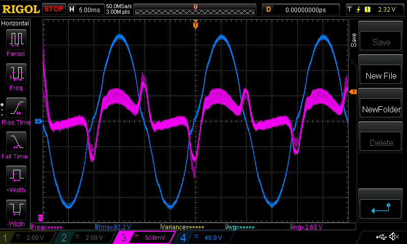 here it is WITHOUT DC balance code, 300W DC + toroid + 3uF 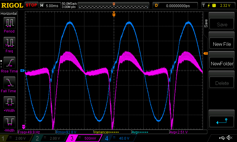 Finally, I noticed that when I switched on the DC balance code, when under the above conditions (300W DC + toroid and the same with or without the 3uF cap) I watched as the DC balance was altered nicely during the bang-bang phase of the closed loop and it looks almost perfect at a certain instance, then it devolves into uncontrolled oscillation which continues indefinitely. So for a second or so, it looks good. see below for good look. 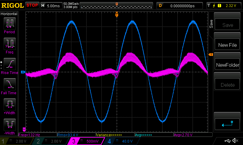 I have made the inverter code send out via the serial port the DC balance correction factor ("i_balance" ) x 100 and I graph it. We can see the linear increase of i_balance during the bang-bang phase and we see it settle OK for a bit then it goes bananas. I have tried different PID control loop factors but it always ends up with uncontrolled oscillation. 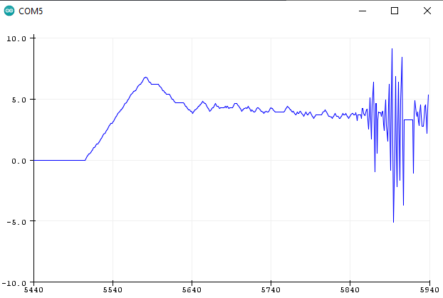 |
||||||
What you are seeing is real. I saw it with the toroids I removed from the dead 3kW Victron inverter. I was curious about this. Just about every photo of our home built toroids have very carefully placed windings that are as evenly spaced as humanly possible to achieve. There is a reason for this and it is to produce some leakage inductance. There is some well developed theory exploring this, as used in power electronics. maybe have a look at https://research.engineering.nyu.edu/power/sites/engineering.nyu.edu.power/files/uploads/leakage%202.pdf |
||||||
.. To verify, the unbalanced load could be disconnected and the large current pulses around zero crossings should still happen. So I did a test. with the DC balance control in effect, 300W DC load + second toroid. it soft starts nicely with the big current spikes. Then the DC balance code starts working, reducing the spikes to very small, then the control loop goes bananas. At this time there are large current spikes at both zero crossings. I then switch off the DC load. Immediately things go quiet, with tiny current peaks at both zero crossings. it goes from this: 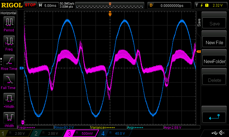 to this when I remove the DC load. Always the DC balance control code is in effect. 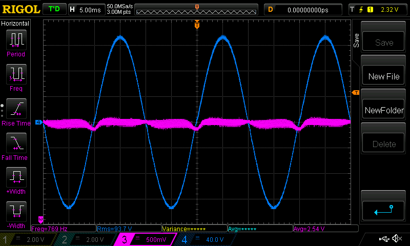 when I disable the DC balance code, those small current peaks disappear too. |
||||||
I am thinking there is something going on. This thing is a increase in current at zero crossings from a CHANGE in AC voltage. I have seen this since forever in the soft start process of all my inverters and I know many people here have seen it too. I can tolerate this short term thing. It not very large current and it only appears for a second or two. But now I think this thing is very much present during the changes to AC voltage that are made by the DC balance code. The current spikes induced by the rapid AC voltage changes, due to the closed loop control of the DC balance scheme are now seen as "DC imbalance" and then they must be corrected for. And the corrections involve fast AC voltage change so that means some more current spike at zero crossing. and the control loop starts chasing it's tail. Surely all I need to do is tune the PID loop? I doubt that this is all that will be needed. This is when I could use a degree in Mathematics. I wonder if I could band-aid over this problem with something like a correction factor that depends on the rate of change of i_balance... The last reply to Wiseguy contains a nice graph of i_balance as it passes through the 3 phases of operation (nice bang-bang, nice pid and bad pid) |
||||||
Changing the ac voltage is a dc offset in a sense, and that needs to be coordinated with the dc bias code to be in phase so to speak. If the voltage is increased only every positive rising edge of one cycle, then increasing the voltage creates a positive cycle bias. Basically the sine wave needs to grow on both the positive and negative sides in progression while maintaining perfect ballance. If you use the same lookup table for both the positive and negative half of the waveform, this is a problem. But if you update the lookup table at 120hz instead of 60, it may not be. Also if your code only computes a fourth of the sine wave, mirrors it, then inverts it: then each time the voltage changes you will also probably produce harmonics |
||||||
Thanks for the link Poida. It is interesting that they stagger the primary and secondary gaps too. I guess that is something to look at if we wind our own transformers. I have done a couple without gaps , they work well but maybe gaps will alleviate some of the extra cost of inductors after the transformer. Pete |
||||||
I assume that you are talking about how to treat saturation not normal ramping. We will also assume that the half wave load is driven during the positive 180° A) If the voltage is increased only every positive rising edge of one cycle, then increasing the voltage creates a positive cycle bias. If you mean only the positive 180° portion is increased over the complete cycle, due to the half wave load, the primary peak voltage for the first 180° is slightly less than before, therefore the core magnetising current is lower, hence a negative voltage magnetising bias is created which we try to cancel by increasing the level of the first 180° magnetising current to be the same as the unloaded negative 180° B) Basically the sine wave needs to grow on both the positive and negative sides in progression while maintaining perfect ballance. We need to do something different - we had balanced cycles then attached a half wave load and started towards saturation the only important consideration to fix, is to keep the core magnetising current exactly equal for each 180°. C)If you use the same lookup table for both the positive and negative half of the waveform, this is a problem. This is not a problem for a resistive load so we agree here, but we need to do something to the positive 180° look up table for the half wave load until the core magnetising current is balanced even if that is done by changing half the look up table. D)But if you update the lookup table at 120hz instead of 60, it may not be. I contend that we need to update each 180° or 120Hz, this should have no effect for balanced loads. E)Also if your code only computes a fourth of the sine wave, mirrors it, then inverts it: then each time the voltage changes you will also probably produce harmonics That description is of a balanced drive for 360° ? If I had a choice between saturation and harmonics I would choose to have harmonics although I don't follow that a brief harmonic event should create a problem. If I am off at a tangent to what you were trying to say, maybe you could describe or explain yourself more. I am not interested so much in being right, only in finding the right solution to avoid the half wave saturation issue. The inverter works great for resistive loads - I am beginning to think the better cure might be to A not use the device or B remove the half wave diode from the offending device and use a 360° triac full wave phase controller to drive the element. I decided to add some more to this post for extra clarity as there still seems to be a bit of confusion. I think mostly to do with the reference to the word "balanced", the PWM can be perfectly balanced, the magnetising current can also be near perfectly balanced both for the no load condition and a resistive load condition. However, for a half wave load condition, whilst the PWM will still be balanced, the magnetising currents are no longer balanced. There are now 2 components contributing to the primary loaded 180° current, one is supplying the half wave load current, this is in addition to the original magnetising current, however the extra current required to supply the half wave load and associated small losses involved, causes slightly less magnetising current. To summarise, the extra current on the loaded 180° causes more resistive losses in the FETs, wiring and high current primary winding to result in less magnetising current for the loaded half cycle, the unloaded half cycle still receives its normal magnetising current (higher than the previous loaded 180°) so we now head towards saturation. Edited 2026-11-06 17:10 by wiseguy |
||||||
I did a test, that was to show the order of events and their timing when I make an abrupt change to the amplitude of one of the half cycles of the AC output. In this test, I reduce the negative AC wave by 0.05, for 2 full 50 Hz cycles. Light Blue is the switch voltage that signals the code to reduce the negative half by 0.05 for 2 full cycles Dark Blue is AC output. Pink is primary current. 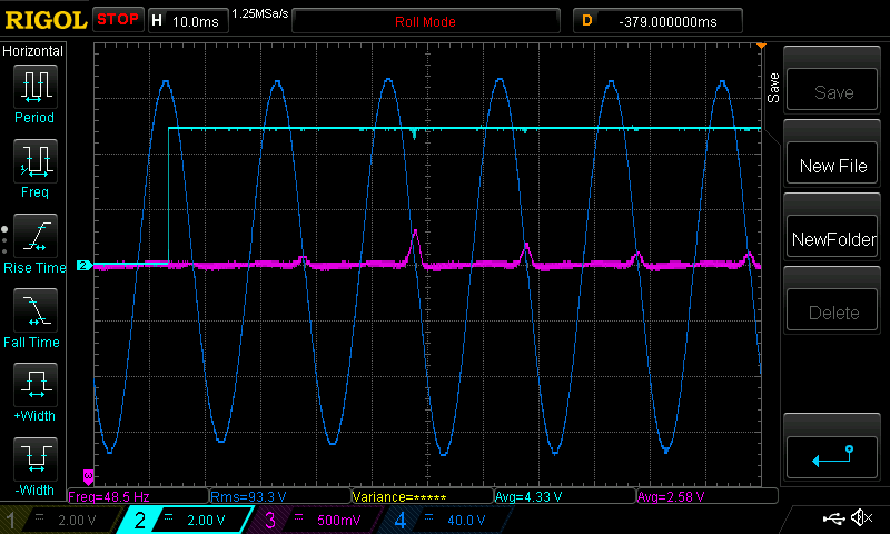 There is a lot of good information in this capture that is immediately applicable to the close loop control programming. 1 and 1/2 time divisions in, the enable switch opens. The next negative half cycle is immediately reduced by 1/5th a division. No current spike yet. We see only 2 of the negative half cycles are reduced in amplitude. The current spike grows to a maximum nearly 2 full cycles AFTER the amplitude change. This delay in primary current increase after an amplitude modification is a major issue in respect to the closed loop control. Additionally, it's clear that making any change to amplitude produces changes in primary current - even with no load running. It is clear to me that my code must now incorporate this delayed response. Ideally my code would run in a loop such as: 1 - measure primary current as both zero crossings 2 - correct these values by removing the increase in current from previous changes made to the amplitude 3 - determine the new change needed to modify the amplitude 4 - apply the change then go back to 1 I could do a few more of these tests to get an idea of how much current increase will result from an various amplitude changes. I expect the time delay to be constant though. This delayed response is why my existing code devolves into unstable oscillation. Edited 2026-11-07 11:15 by poida |
||||||
Yes, that would make sense. The inductive time-constant is: Tc = L / R. Below saturation L is fairly constant and R (total primary circuit resistance) also doesn't change much. The size of the PWM change should affect the size of the DC offset but not the delay. R is very low so a Tc of several cycles seems reasonable. |
||||||
Okay, the half-wave load turn off effect on the load side transformer magnetizing current is expected but perhaps not quite the magnitude. The current pulses disappearing after disabling the imbalance compensation suggests perhaps there should be a minimum imbalance threshold for applying imbalance compensation? |
||||||
Perhaps you could also try adding deadtime to the imbalance PID loop. So, the deadtime (1.5 cycles?) would be activated everytime a non-zero imbalance compensation is applied. During the deadtime no imbalance compensation is applied but sampling continues. I suspect the findings would only be accurate for your particular inverter and environment. It's basically trying to determine the inverter's local grid impedance? Edited 2026-11-08 05:57 by analog8484 |
||||||
Analog848, I think you are understanding what is going on far better than me. I agree the idea of working out how much effect rises from various AC amplitude imbalances is pointless. I like the idea of dead time though. Once an adjustment is made, I wait something like 5 or 10 half cycles to allow the impulse of the sudden change to dissipate to a large degree. Then examine the DC balance and calculate a new adjustment. This will result in a slower response but it could remove the feedback thing that results in oscillation. I will try this now. |
||||||
deadtime results so far: PID values P = 6, I = 0.1, D = 0.3, gain 1e-5 (the PID settings used in nearly all previous tests) deadtime 5, 10 and 20 all bad oscillation I found I could get far nicer results and no oscillation with PID values P=6, I = 1, d = 0.0, gain 1e-5 deadtime 5 or 10 no oscillation. This is with the second toroid in circuit. When I remove it, using the last test config above and alter the ADC offset for the current sensor zero current output to now be 522 (not 512 as in the ideal world and not 516 as used in all past tests) I get this perfection here: 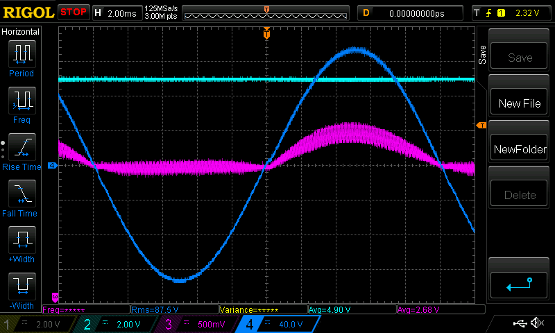 the plot of i_balance looks different now. the steps are due to deadtime. the plot is updated at 100Hz and with DT = 10, we see about 10 steps for 100 samples (or 1 second) 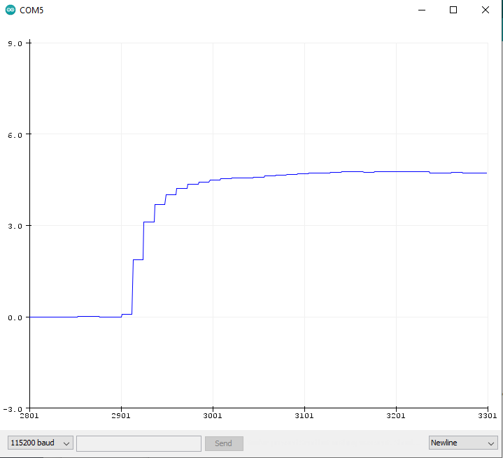 for anyone interested, here is the latest code It runs on the picoverter board. oneFET_half_wave_correction_v3.zip Edited 2026-11-08 14:54 by poida |
||||||
Thanks for the quick work poida. The improved behavior looks very nice. Glad to see the deadtime helped. I suggested using deadtime based on my experience screwing around with PID temperature control which has a much slower physical process delay. I see you also set D element to 0 to get the improved behavior. That's consistent with my experience with non-zero D element at least in standard PID. Generally, I've only found using a D element helpful in compensation when it's very small and updated on a much slower time scale using longer time average relative to the PI elements. So, it's not really standard PID. |
||||||
Peter the waveform for the unbalanced load looks essentially perfect. I hope you can indulge me some clarification on various aspects of the cure as it stands. A) Can we see a CRO shot of what happens at the immediate application of the half wave load - I have a picture in my mind of seeing saturation areas, that diminish towards stability after a period of cycles? B) What is the essential mechanism now to bring about the stability, do we increase the peak amplitude of the loaded 180° or reduce the amplitude of the unloaded 180°? C) Can I assume the RMS AC voltage is restored back to its original value after the half wave was applied - this has implications with B above. D) Is the cure load dependent as it stands, ie will it work the same for 50W to 1KW ? I just want to better understand the status of where we currently are. Maybe these are early days needing more work or maybe you have found the holy grail ? Thanks for your continued efforts & input - you must be pretty chuffed at these last results? |
||||||
Mike, A - see this. it takes about 30 or so cycles to respond to the change from full wave resistive load to 1/2 wave resistive load. This is due to the slow response of the PID control. 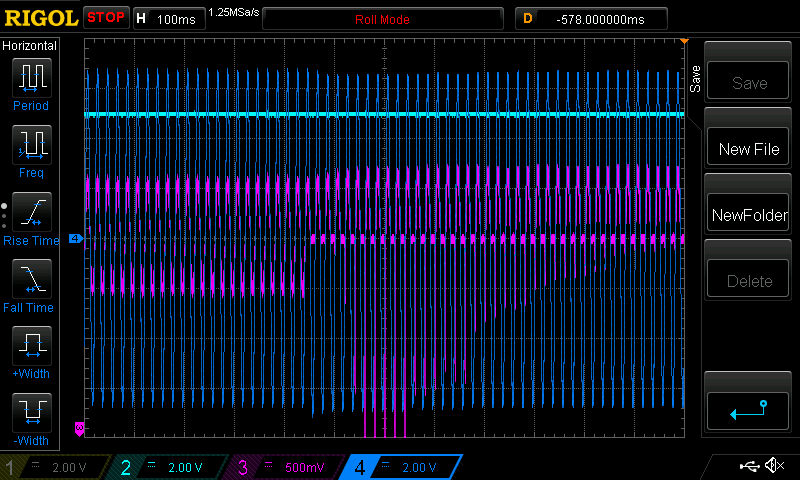 B - The code looks for saturation on one or the other 1/2 cycle and reduces the amplitude of the voltage for that half cycle. if the negative part of the waveform has the saturation peaks, I reduce it's amplitude. Or if the positive part has the saturation, I reduce it's amplitude. The code measures DC current at zero crossing for both negative part and positive part and keeps both values separate. In my code I call one 1/2 of the waveform to be output from "V1" and the other half will be output from "V2" V1 and V2 are the 2 outputs we connect wires that go to the primary winding and choke. Always the AC voltage output control loop is ensuring that it sees the setpoint and increases or decreases the main control factor to suit. The AC output is seen on the Dark Blue trace I have noticed that with a full wave load the PWM is 466 clocks for both 1/2 waves. then when I switch in the diode, it becomes 441 and 468 for the 1/2 waves. I suppose a small increase in output voltage is now required to get the "240V AC" output. C- yes. Always there is the main AC output control loop running and working to obtain the required AC output. (see B answer) D- as far as I can test with 100W up to 400W it works fine. at 100W: AC load 450 for V1, 450 for V2 DC load 451 for V1, 440 for V2 at 400W: AC load 465 for V1, 465 for V2 DC load 468 for V1, 441 for V2 These are PWM maximum pulse width factors, and can be used as an indication of the maximum AC modulation AKA max AC voltage. For the 100W load only a little adjustment was needed, only 10 clocks reduction. For the 400W load a bit more reduction needed, 24 clocks. With a 800 clock PWM cycle, this is about 1.25% reduction for 100W load and 3.12% for the 400W load. This is not a lot of reduction on the half wave amplitude. The main reason it looks so good is due to adjusting the zero offset of the DC current sensor. The previous post had me say I change it from 516 to 522. (the ADC returns values from 0 to 1023 and if the sensor and ADC was perfect the zero current value "should" be 512 but it is not) Changing this zero offset made a huge difference to the niceness of the results. 100W DC load 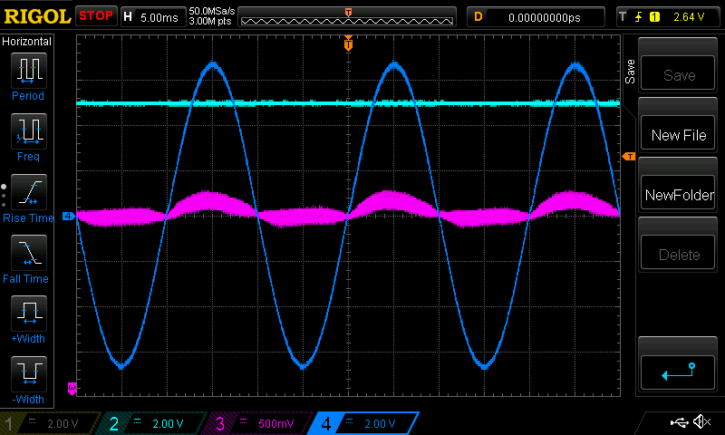 and 400W load 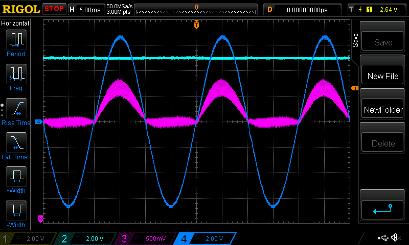 It's funny to me now that I do not care much how fast it responds to changes rather I am more interested in how accurately it responds to and settles down to a steady state with no sharp peaks in primary current I have hard limits in the code to ensure one or the other 1/2 wave is not reduced more than 20% and this seems to be more than enough for loads up to 1kW or even more. Edited 2026-11-12 21:19 by poida |
||||||
Thanks for the tests and posting the results. I will mull it all over for a while. |
||||||
Was 516 determined based on some previous calibration? Or it was a guesstimate? I am wondering if and why the actual zero offset changed? |
||||||
516 was chosen as a starting point when I first did some testing. I found it near enough. Over time I think the zero point changed a little. The LEM current sensors do drift, mainly after copping a large current pulse which then alters the zero point in a sort of permanent way. Once I had stable code and some understanding of what was going on, it was time to fine tune it a bit. Even 2 ADC counts change made a clearly visible change to the settled state's current blip. I find working with these sensors easy and I trust their output (I know what it looks like when they are overloaded and know the zero set point changes around a bit) In my view now is not the time to worry about this sort of thing since I am not presenting a completed project with parts list. I am showing results of experimentation and a simple to use sensor is ideal for my needs. I wonder if there could be a self zeroing primary current signal design that might be used when we build inverters incorporating this control? Maybe using sample and hold function, a differential amp, a common signal source,etc. that does have a zero offset but it is subtracted out to nil from the diff amp. |
||||||
I just did a test with a larger load. The Hair Drier.. full load, no diode in circuit: V1 500 , V2 500 (i.e. balanced AC), 1130 W DC input with diode in circuit: V1 445, V2 500 and about 580W DC input it looks like this: 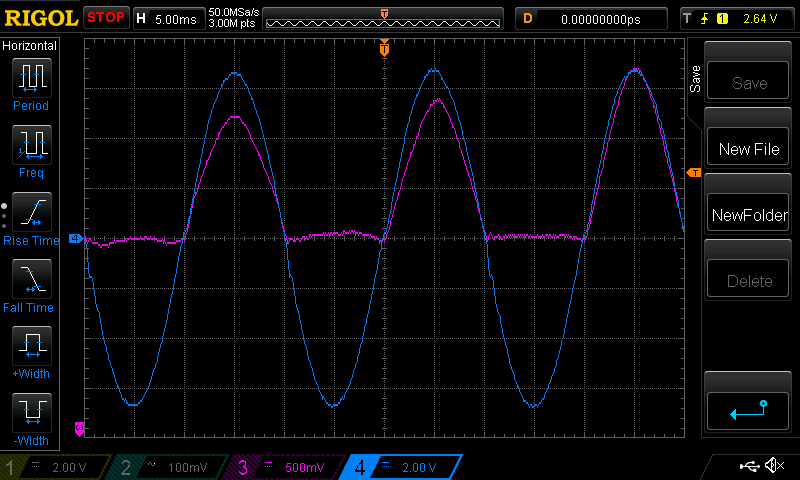 the 55 clock adjustment, reducing V1 amplitude is 6.8% for some reason the hair drier applies a variable load, pulling differing amount of current from cycle to cycle. This is a few cycles without the diode in circuit. 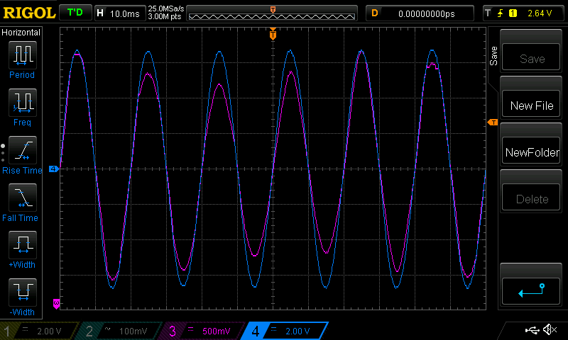 |
||||||
| Page 5 of 6 |
||||||
 |
The Back Shed's forum code is written, and hosted, in Australia. |


